IDT72V3622 Ver la hoja de datos (PDF) - Integrated Device Technology
Número de pieza
componentes Descripción
Lista de partido
IDT72V3622
Integrated Device Technology

IDT72V3622 Datasheet PDF : 29 Pages
| |||
IDT72V3622/72V3632/72V3642 CMOS 3.3V SyncBiFIFOTM
256 x 36 x 2, 512 x 36 x 2, 1,024 x 36 x 2
COMMERCIAL TEMPERATURE RANGE
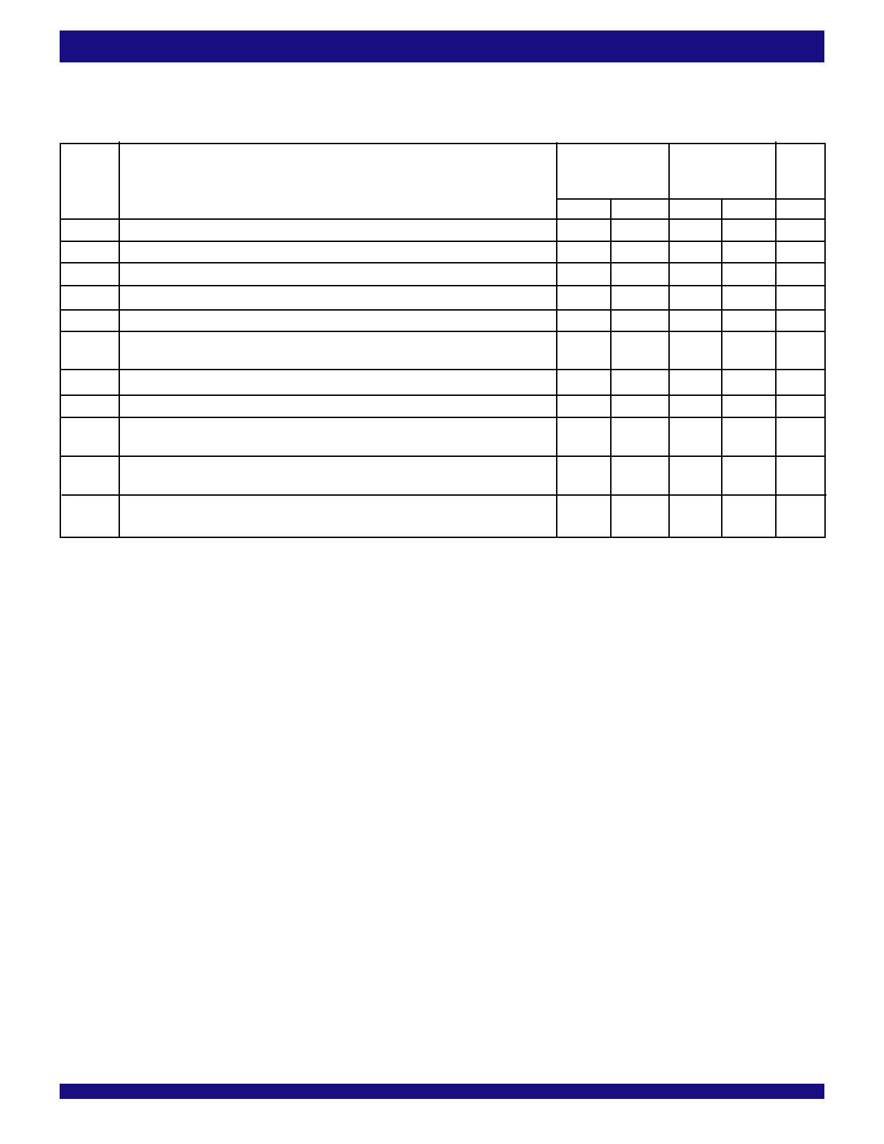
SWITCHING CHARACTERISTICS OVER RECOMMENDED RANGES O. SUPPLY
VOLTAGE AND OPERATING .REE-AIR TEMPERATURE, CL = 30 p.
Commercial: VCC=3.3V± 0.30V; for 10ns (100 MHz) operation, VCC=3.3V ±0.15V; TA = 0ο C to +70ο C; JEDEC JESD8-A compliant
Symbol
Parameter
tA
Access Time, CLKA↑ to A0-A35 and CLKB↑ to B0-B35
tWEF Propagation Delay Time, CLKA↑ to FFA/IRA and CLKB↑ to FFB/IRB
tREF Propagation Delay Time, CLKA↑ to EFA/ORA and CLKB↑ to EFB/ORB
tPAE Propagation Delay Time, CLKA↑ to AEA and CLKB↑ to AEB
tPAF Propagation Delay Time, CLKA↑ to AFA and CLKB↑ to AFB
tPMF Propagation Delay Time, CLKA↑ to MBF1 LOW or MBF2 HIGH and CLKB↑ to
MBF2 LOW or MBF1 HIGH
tPMR Propagation Delay Time, CLKA↑ to B0-B35(2) and CLKB↑ to A0-A35(3)
tMDV Propagation Delay Time, MBA to A0-A35 valid and MBB to B0-B35 Valid
tRSF Propagation Delay Time, RST1 LOW to AEB LOW, AFA HIGH, and MBF1 HIGH,
and RST2 LOW to AEA LOW, AFB HIGH, and MBF2 HIGH
tEN
Enable Time, CSA and W/RA LOW to A0-A35 Active and CSB LOW and W/RB
HIGH to B0-B35 Active
tDIS Disable Time, CSA or W/RA HIGH to A0-A35 at high-impedance and CSB HIGH or
W/RB LOW to B0-B35 at high-impedance
NOTES:
1. For 10ns speed grade only: VCC = 3.3V +/- 0.15V, TA = 0° to +70°C; JEDEC JESD8-A compliant.
2. Writing data to the mail1 register when the B0-B35 outputs are active and MBB is HIGH.
3. Writing data to the mail2 register when the A0-A35 outputs are active and MBA is HIGH.
4. Industrial temperature range is available by special order.
IDT72V3622L10(1) IDT72V3622L15
IDT72V3632L10(1) IDT72V3632L15
IDT72V3642L10(1) IDT72V3642L15
Min. Max. Min. Max. Unit
2
6.5
2
10
ns
2
6.5
2
8
ns
1
6.5
1
8
ns
1
6.5
1
8
ns
1
6.5
1
8
ns
0
6.5
0
8
ns
2
8
2
10
ns
2
6.5
2
10
ns
1
10
1
15
ns
2
6
2
10
ns
1
6
1
8
ns
9
Share Link: