IRF620 Ver la hoja de datos (PDF) - Vishay Semiconductors
Número de pieza
componentes Descripción
Lista de partido
IRF620 Datasheet PDF : 9 Pages
| |||
IRF620, SiHF620
Vishay Siliconix
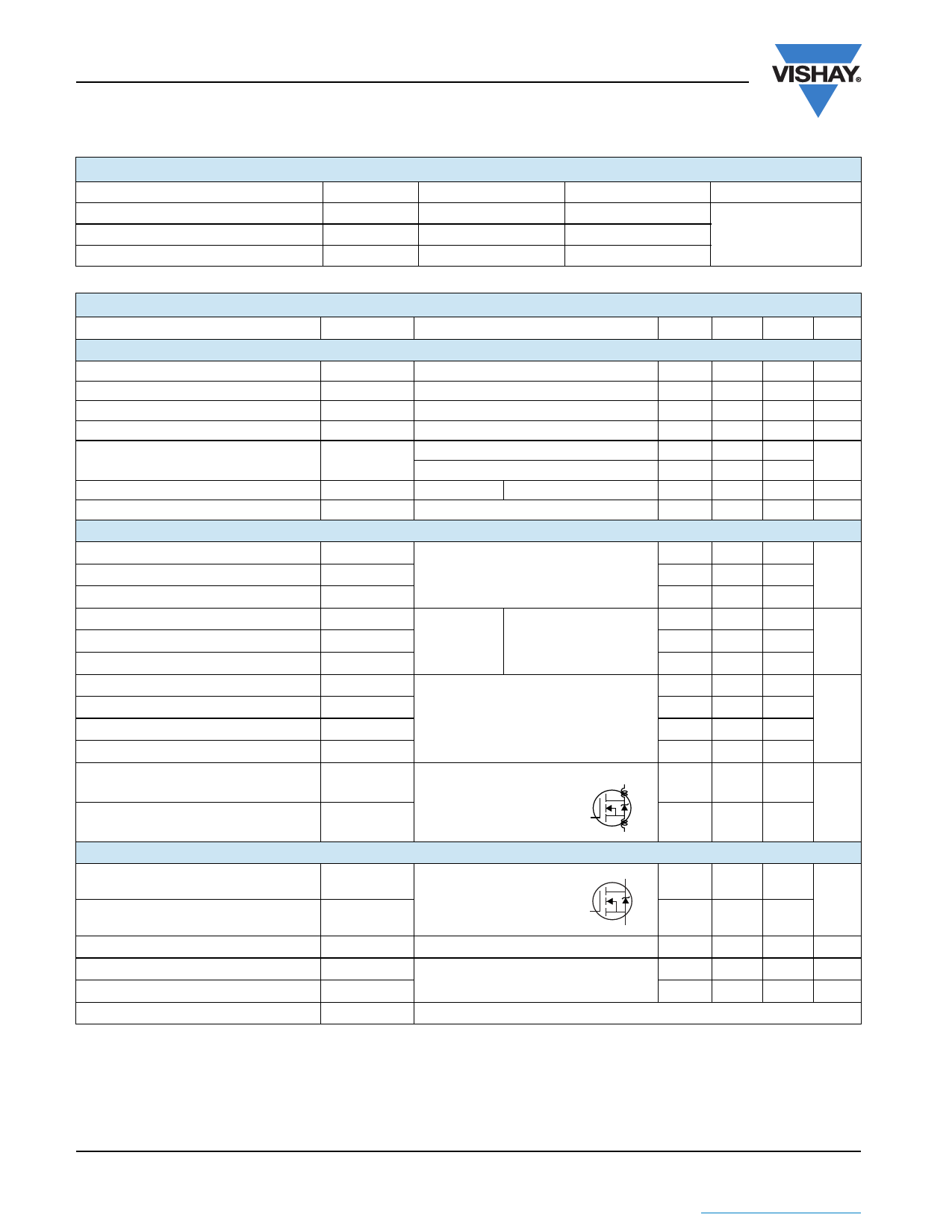
THERMAL RESISTANCE RATINGS
PARAMETER
SYMBOL
Maximum Junction-to-Ambient
Case-to-Sink, Flat, Greased Surface
Maximum Junction-to-Case (Drain)
RthJA
RthCS
RthJC
TYP.
-
0.50
-
MAX.
62
-
2.5
UNIT
°C/W
SPECIFICATIONS (TJ = 25 °C, unless otherwise noted)
PARAMETER
SYMBOL
TEST CONDITIONS
Static
Drain-Source Breakdown Voltage
VDS Temperature Coefficient
Gate-Source Threshold Voltage
Gate-Source Leakage
Zero Gate Voltage Drain Current
Drain-Source On-State Resistance
Forward Transconductance
Dynamic
VDS
VDS/TJ
VGS(th)
IGSS
IDSS
RDS(on)
gfs
VGS = 0 V, ID = 250 μA
Reference to 25 °C, ID = 1 mA
VDS = VGS, ID = 250 μA
VGS = ± 20 V
VDS = 200 V, VGS = 0 V
VDS = 160 V, VGS = 0 V, TJ = 125 °C
VGS = 10 V
ID = 3.1 Ab
VDS = 50 V, ID = 3.1 A
Input Capacitance
Output Capacitance
Reverse Transfer Capacitance
Total Gate Charge
Gate-Source Charge
Gate-Drain Charge
Turn-On Delay Time
Rise Time
Turn-Off Delay Time
Fall Time
Ciss
Coss
Crss
Qg
Qgs
Qgd
td(on)
tr
td(off)
tf
VGS = 0 V,
VDS = 25 V,
f = 1.0 MHz, see fig. 5
VGS = 10 V
ID = 4.8 A, VDS = 160 V,
see fig. 6 and 13b
VDD = 100 V, ID = 4.8 A,
Rg = 18 , RD = 20 , see fig. 10b
MIN.
200
-
2.0
-
-
-
-
1.5
-
-
-
-
-
-
-
-
-
-
TYP. MAX. UNIT
-
-
V
0.29
-
V/°C
-
4.0
V
-
± 100 nA
-
25
μA
-
250
-
0.80
-
-
S
260
-
100
-
pF
30
-
-
14
-
3.0
nC
-
7.9
7.2
-
22
-
ns
19
-
13
-
Internal Drain Inductance
LD
Internal Source Inductance
LS
Drain-Source Body Diode Characteristics
Continuous Source-Drain Diode Current
IS
Pulsed Diode Forward Currenta
ISM
Between lead,
6 mm (0.25") from
package and center of
die contact
MOSFET symbol
showing the
integral reverse
p - n junction diode
D
G
S
D
G
S
-
4.5
-
nH
-
7.5
-
-
-
5.2
A
-
-
18
Body Diode Voltage
VSD
TJ = 25 °C, IS = 5.2 A, VGS = 0 Vb
-
-
1.8
V
Body Diode Reverse Recovery Time
trr
-
150
300
ns
TJ = 25 °C, IF = 4.8 A, dI/dt = 100 A/s
Body Diode Reverse Recovery Charge
Qrr
-
0.91 1.8
μC
Forward Turn-On Time
ton
Intrinsic turn-on time is negligible (turn-on is dominated by LS and LD)
Notes
a. Repetitive rating; pulse width limited by maximum junction temperature (see fig. 11).
b. Pulse width 300 μs; duty cycle 2 %.
www.vishay.com
2
Document Number: 91027
S11-0510-Rev. B, 21-Mar-11
This datasheet is subject to change without notice.
THE PRODUCT DESCRIBED HEREIN AND THIS DATASHEET ARE SUBJECT TO SPECIFIC DISCLAIMERS, SET FORTH AT www.vishay.com/doc?91000
Share Link: 