LAN9117 Ver la hoja de datos (PDF) - SMSC -> Microchip
Número de pieza
componentes Descripción
Lista de partido
LAN9117 Datasheet PDF : 131 Pages
| |||
High Performance Single-Chip 10/100 Non-PCI Ethernet Controller
Datasheet
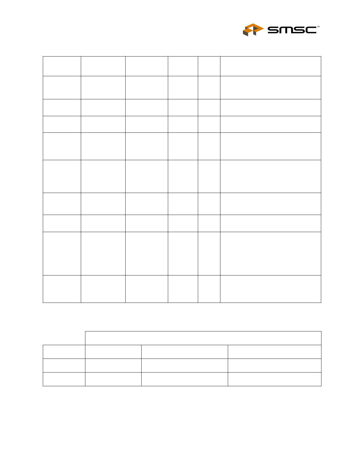
Table 2.1 Host Bus Interface Signals
PIN NO.
43-46,49-
53,56-59,62-
64
12-18
NAME
Host Data
Host Address
92
Read Strobe
93
Write Strobe
94
Chip Select
72
71,73,84,90,
91
74
Interrupt
Request
Reserved
10/100
Selector
76
FIFO Select
SYMBOL
D[15:0]
BUFFER
#
TYPE PINS
DESCRIPTION
I/O8
16 Bi-directional data port. Supports
Big/Little Endian Byte ordering.
A[7:1]
nRD
nWR
nCS
IRQ
Reserved
IS
IS
IS
IS
O8/OD8
7 7-bit Address Port. Used to select
Internal CSR’s and TX and RX FIFOs.
1 Active low strobe to indicate a read
cycle.
1 Active low strobe to indicate a write
cycle. This signal, qualified with nCS, is
also used to wakeup the LAN9117
when it is in a reduced power state.
1 Active low signal used to qualify read
and write operations. This signal
qualified with nWR is also used to
wakeup the LAN9117 when it is in a
reduced power state.
1 Programmable Interrupt request.
Programmable polarity, source and
buffer types.
5 No Connect
SPEED_SEL I (PU)
FIFO_SEL
IS
1 This signal functions as a configuration
input on power-up and is used to select
the default Ethernet settings. Upon
deassertion of reset, the value of the
input is latched. This signal functions
as shown in Table 2.2, "Default
Ethernet Settings", below.
1 When driven high all accesses to the
LAN9117 are to the RX or TX Data
FIFOs. In this mode, the A[7:3] upper
address inputs are ignored.
SPEED_SEL
0
1
Table 2.2 Default Ethernet Settings
DEFAULT ETHERNET SETTINGS
SPEED
DUPLEX
10MBPS
HALF-DUPLEX
100MBPS
HALF-DUPLEX
AUTO NEG.
DISABLED
ENABLED
SMSC LAN9117
15
DATASHEET
Revision 1.1 (05-17-05)
Share Link: 