LT1964 Ver la hoja de datos (PDF) - Linear Technology
Número de pieza
componentes Descripción
Lista de partido
LT1964 Datasheet PDF : 12 Pages
| |||
LT1964
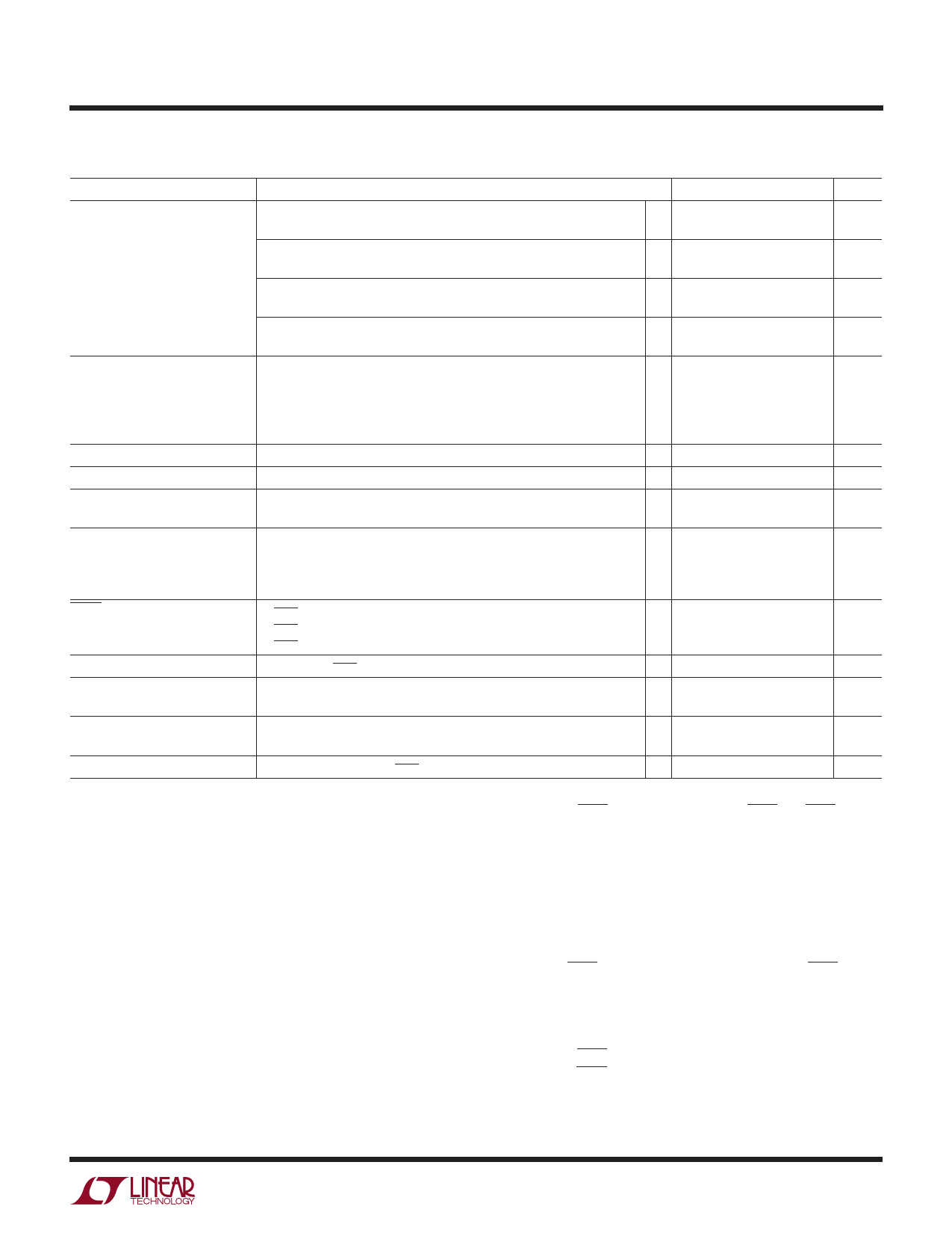
ELECTRICAL CHARACTERISTICS The q denotes the specifications which apply over the full operating
temperature range, otherwise specifications are at TA = 25°C.
PARAMETER
CONDITIONS
MIN TYP MAX UNITS
Dropout Voltage
VIN = VOUT(NOMINAL)
(Notes 4, 5)
GND Pin Current
VIN = VOUT(NOMINAL)
(Notes 4, 6)
Output Voltage Noise
ADJ Pin Bias Current
ILOAD = – 1mA
ILOAD = – 1mA
q
ILOAD = – 10mA
ILOAD = – 10mA
q
ILOAD = – 100mA
ILOAD = – 100mA
q
ILOAD = – 200mA
ILOAD = – 200mA
q
ILOAD = 0mA
q
ILOAD = – 1mA
q
ILOAD = – 10mA
q
ILOAD = – 100mA
q
ILOAD = – 200mA
q
COUT = 10µF, CBYP = 0.01µF, ILOAD = –200mA, BW = 10Hz to 100kHz
(Notes 2, 7)
0.1 0.15
V
0.19
V
0.15 0.20
V
0.25
V
0.26 0.33
V
0.39
V
0.34 0.42
V
0.49
V
30
70
µA
85
180
µA
300 600
µA
1.3
3
mA
2.5
6
mA
30
µVRMS
30
100
nA
Minimum Input Voltage (Note 12)
ILOAD = –200mA
Shutdown Threshold
SHDN Pin Current (Note 8)
Quiescent Current in Shutdown
Ripple Rejection
Current Limit
Input Reverse Leakage Current
LT1964-BYP
LT1964-SD
VOUT = Off to On (Positive)
VOUT = Off to On (Negative)
VOUT = On to Off (Positive)
VOUT = On to Off (Negative)
VSHDN = 0V
VSHDN = 15V
VSHDN = –15V
VIN = –6V, VSHDN = 0V
VIN – VOUT = –1.5V(Avg), VRIPPLE = 0.5VP-P,
fRIPPLE = 120Hz, ILOAD = –200mA
VIN = –6V, VOUT = 0V
VIN = VOUT(NOMINAL) –1.5V, ∆VOUT = 0.1V
VIN = 20V, VOUT, VADJ, VSHDN = Open Circuit
q
–1.9 –2.8
V
q
–1.6 –2.2
V
q
1.6
2.1
V
q
–1.9 –2.8
V
q 0.25 0.8
V
q –0.25 –0.8
V
–1
±0.1
1
µA
6
15
µA
–3
–9
µA
q
3
10
µA
46
54
dB
350
mA
q 220
mA
q
1
mA
Note 1: Absolute Maximum Ratings are those values beyond which the life
of a device may be impaired.
Note 2: The LT1964 (adjustable version) is tested and specified for these
conditions with the ADJ pin connected to the OUT pin.
Note 3: Operating conditions are limited by maximum junction
temperature. The regulated output voltage specification will not apply for
all possible combinations of input voltage and output current. When
operating at maximum input voltage, the output current range must be
limited. When operating at maximum output current, the input voltage
range must be limited.
Note 4: To satisfy requirements for minimum input voltage, the LT1964
(adjustable version) is tested and specified for these conditions with an
external resistor divider (two 249k resistors) for an output voltage of
–2.44V. The external resistor divider will add a 5µA DC load on the output.
Note 5: Dropout voltage is the minimum input to output voltage differential
needed to maintain regulation at a specified output current. In dropout, the
output voltage will be equal to: (VIN + VDROPOUT).
Note 6: GND pin current is tested with VIN = VOUT(NOMINAL) and a current
source load. This means the device is tested while operating in its dropout
region. This is the worst-case GND pin current. The GND pin current will
decrease slightly at higher input voltages.
Note 7: ADJ pin bias current flows out of the ADJ pin.
Note 8: Positive SHDN pin current flows into the SHDN pin. SHDN pin
current is included in the GND pin current specification.
Note 9: For input-to-output differential voltages greater than 7V, a 50µA
load is needed to maintain regulation.
Note 10: The LT1964E is guaranteed to meet performance specifications
from 0°C to 125°C. Specifications over the –40°C to 125°C operating
junction temperature range are assured by design, characterization and
correlation with statistical process controls.
Note 11: A parasitic diode exists internally on the LT1964 between the
OUT, ADJ and SHDN pins and the IN pin. The OUT, ADJ and SHDN pins
cannot be pulled more than 0.5V more negative than the IN pin during
fault conditions, and must remain at a voltage more positive than the IN
pin during operation.
Note 12: For the LT1964-BYP, this specification accounts for the operating
threshold of the SHDN pin, which is tied to the IN pin internally. For the
LT1964-SD, the SHDN threshold must be met to ensure device operation.
Note 13: Actual thermal resistance (θJA) junction to ambient will be a
function of board layout. Junction-to-case thermal resistance (θJC)
measured at Pin 2 is 60°C/W. See the Thermal Considerations section in
the Applications Information.
1964f
3
Share Link: 