LT3029 Ver la hoja de datos (PDF) - Linear Technology
Número de pieza
componentes Descripción
Lista de partido
LT3029 Datasheet PDF : 20 Pages
| |||
LT3029
APPLICATIONS INFORMATION
The LT3029 is a dual 500mA/500mA low dropout regulator
with independent inputs, micropower quiescent current
and shutdown. The device supplies up to 500mA from each
channel’s output at a typical dropout voltage of 300mV.
The two regulators share a common GND pin and are
thermally coupled. However, the two inputs and outputs of
the LT3029 operate independently. Each channel can be
shut down independently, but a thermal shutdown fault
on either channel shuts off the output on both channels.
The addition of a 10nF reference bypass capacitor lowers
output voltage noise to 20μVRMS over a 10Hz to 100kHz
bandwidth. Additionally, the reference bypass capacitor
improves transient response of the regulator, lowering
the settling time for transient load conditions. The low
operating quiescent current (55μA per channel) drops to
less than 1μA in shutdown. In addition to the low quies-
cent current, the LT3029 regulator incorporates several
protection features that make it ideal for use in battery-
powered systems. Most importantly, the device protects
itself against reverse input voltages. Current limiting with
foldback necessitates a minimum load current of 20μA
for input/output voltage differentials of more than 10V to
keep the output regulated.
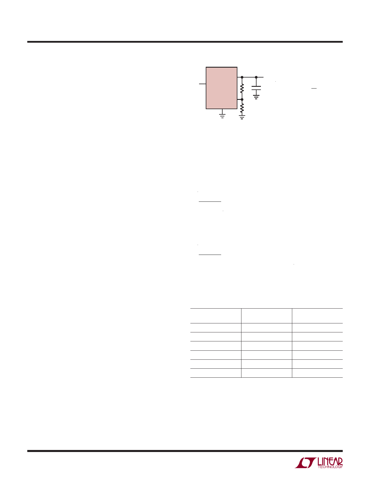
Adjustable Operation
Each of the LT3029’s channels has an output voltage range
of 1.215V to 19.5V. Figure 1 illustrates that output voltage
is set by the ratio of two external resistors. The device
regulates the output to maintain the corresponding ADJ
pin voltage at 1.215V referenced to ground. R1’s current
equals 1.215V/R1. R2’s current equals R1’s current plus
the ADJ pin bias current. The ADJ pin bias current, 30nA at
25°C, flows through R2 into the ADJ pin. Use the formula
in Figure 1 to calculate output voltage. Linear Technology
recommends that the value of R1 be less than 243k to
minimize errors in the output voltage due to the ADJ pin bias
current. In shutdown, the output turns off and the divider
current is zero. Curves of ADJ Pin Voltage vs Temperature
and ADJ Pin Bias Current vs Temperature appear in the
Typical Performance Characteristics section.
LT3029
OUT1/OUT2
VIN
IN1/IN2
R2
VOUT
C
( ) VOUT
=
1.215V
⎛
⎝⎜
1+
R2 ⎞
R1⎠⎟
+
IADJ
(R2)
ADJ1/ADJ2
GND
R1
VADJ = 1.215V
IADJ = 30nA AT 25°C
OUTPUT RANGE = 1.215V TO 19.5V
3029 F01
Figure 1. Adjustable Operation
Linear Technology tests and specifies each LT3029 channel
with its ADJ pin tied to the corresponding OUT pin for a
1.215V output voltage. Specifications for output voltages
greater than 1.215V are proportional to the ratio of desired
output voltage to 1.215V:
VOUT
1.215V
For example, load regulation on either output for an output
current change of 1mA to 500mA is typically –2.5mV at
VOUT = 1.215V. At VOUT = 2.5V, load regulation is:
2.5V • (−2.5mV) = − 5.14mV
1.215V
Table 1 shows 1% resistor divider values for some com-
mon output voltages with a resistor divider current of
approximately 5μA.
Table 1. Output Voltage Resistor Divider Values
VOUT
R1
R2
(V)
(k)
(k)
1.5
237
54.9
1.8
237
113
2.5
243
255
3
232
340
3.3
210
357
5
200
619
3029fa
12
Share Link: 