LT3029 Ver la hoja de datos (PDF) - Linear Technology
Número de pieza
componentes Descripción
Lista de partido
LT3029 Datasheet PDF : 20 Pages
| |||
LT3029
APPLICATIONS INFORMATION
The LT3029 incurs no damage if either ADJ pin is pulled
above or below ground by 9V. If the input is left open
circuit or grounded, the ADJ pins perform like an open
circuit down to –1.5V, and then like a 1.2k resistor down
to –9V when pulled below ground. When pulled above
ground, the ADJ pins perform like an open circuit up to
0.5V, then like a 5.7k resistor up to 3V, then like a 1.8k
resistor up to 9V.
In situations where an ADJ pin connects to a resistor
divider that would pull the pin above its 9V clamp volt-
age if the output is pulled high, the ADJ pin input current
must be limited to less than 5mA. For example, assume
a resistor divider sets the regulated output voltage to
1.5V, and the output is forced to 20V. The top resistor of
the resistor divider must be chosen to limit the current
into the ADJ pin to less than 5mA when the ADJ pin is
at 9V. The 11V difference between the OUT and ADJ pins
divided by the 5mA maximum current into the ADJ pin
yields a minimum top resistor value of 2.2k.
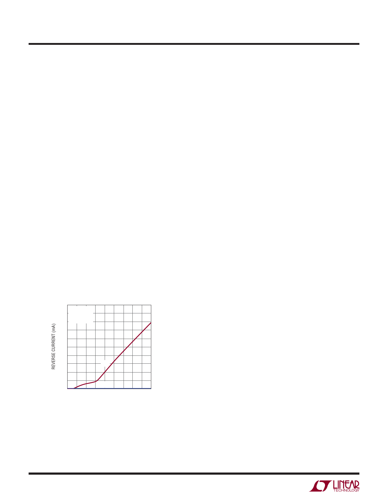
In circuits where a backup battery is required, several
different input/output conditions can occur. The output
voltage may be held up while the input is either pulled
to ground, pulled to some intermediate voltage or is left
open-circuit. Current flow back into the output follows the
curve shown in Figure 5.
5.0
TJ = 25°C
4.5 VIN = 0V
4.0 VADJ = VOUT
3.5
3.0
2.5
2.0
1.5
IADJ
1.0
0.5
IOUT
0
012345678
OUTPUT VOLTAGE (V)
IADJ FLOWS INTO ADJ PIN TO GND PIN
IOUT FLOWS INTO OUT PIN TO IN PIN
9
3029 F05
Figure 5. Reverse Output Current
If either of the LT3029’s IN pins is forced below its cor-
responding OUT pin, or the OUT pin is pulled above its
corresponding IN pin, input current for that channel typi-
cally drops to less than 2μA. This occurs if the IN pin is
connected to a discharged (low voltage) battery, and either
a backup battery or a second regulator circuit holds up
the output. The state of that channel’s SHDN pin has no
effect on the reverse output current if the output is pulled
above the input.
Overload Recovery
Like many IC power regulators, the LT3029 has safe
operating area (SOA) protection. The safe area protec-
tion decreases current limit as input-to-output voltage
increases and keeps the power transistor inside a safe
operating region for all values of input-to-output voltage.
The protective design provides some output current at
all values of input-to-output voltage up to the specified
maximum operational input voltage of 20V.
When power is first applied, as input voltage rises, the
output follows the input, allowing the regulator to start-up
into very heavy loads. During start-up, as the input voltage
is rising, the input-to-output voltage differential is small,
allowing the regulator to supply large output currents.
With a high input voltage, an event can occur wherein
removal of an output short will not allow the output to
recover. The event occurs with a heavy output load when
the input voltage is high and the output voltage is low.
Common situations occur immediately after the removal
of a short-circuit or if the shutdown pin is pulled high after
the input voltage has already been turned on. The load line
intersects the output current curve at two points creating
two stable output operating points for the regulator. With
this double intersection, the input power supply may need
to be cycled down to zero and brought up again to make
the output recover.
3029fa
16
Share Link: 