LTC2202I(RevB) Ver la hoja de datos (PDF) - Linear Technology
Número de pieza
componentes Descripción
Lista de partido
LTC2202I Datasheet PDF : 32 Pages
| |||
LTC2203/LTC2202
ABSOLUTE AXI U RATI GS
OVDD = VDD (Notes 1 and 2)
Supply Voltage (VDD)................................... –0.3V to 4V
Digital Output Supply Voltage (OVDD).......... –0.3V to 4V
Digital Output Ground Voltage (OGND)........ –0.3V to 1V
Analog Input Voltage (Note 3) ..... –0.3V to (VDD + 0.3V)
Digital Input Voltage .................... –0.3V to (VDD + 0.3V)
Digital Output Voltage................ –0.3V to (OVDD + 0.3V)
Power Dissipation............................................ 2000mW
Operating Temperature Range
LTC2203C/LTC2202C............................... 0°C to 70°C
LTC2203I/LTC2202I .............................–40°C to 85°C
Storage Temperature Range ..................– 65°C to 125°C
UW U
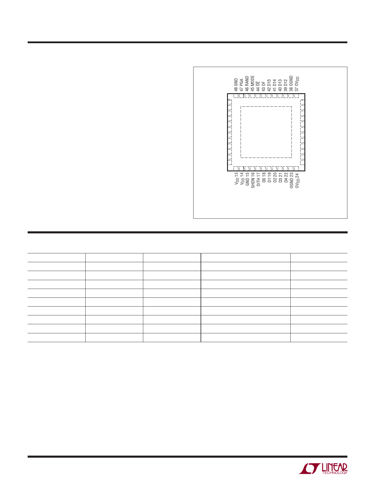
PACKAGE/ORDER I FOR ATIO
TOP VIEW
SENSE 1
VCM 2
VDD 3
VDD 4
GND 5
AIN+ 6
AIN– 7
49
GND 8
GND 9
CLK 10
GND 11
VDD 12
36 OVDD
35 D11
34 D10
33 D9
32 D8
31 OGND
30 CLKOUT+
29 CLKOUT–
28 D7
27 D6
26 D5
25 OVDD
UK PACKAGE
48-LEAD (7mm × 7mm) PLASTIC QFN
EXPOSED PAD IS GND (PIN 49)
MUST BE SOLDERED TO PCB BOARD
TJMAX = 125°C, θJA = 29°C/W
TJMAX = 150°C, OPTION AVAILABLE, CONSULT FACTORY
ORDER PART
NUMBER
UK PART*
MARKING
LTC2203CUK
LTC2202CUK
LTC2203IUK
LTC2202IUK
LTC2203UK
LTC2202UK
LTC2203UK
LTC2202UK
Order Options Tape and Reel: Add #TR
Lead Free: Add #PBF Lead Free Tape and Reel: Add #TRPBF
Lead Free Part Marking: http://www.linear.com/leadfree/
*The temperature grade is identified by a label on the shipping container.
Consult LTC Marketing for parts specified with wider operating temperature ranges.
CO VERTER CHARACTERISTICS The ● denotes the specifications which apply over the full operating
temperature range, otherwise specifications are at TA = 25°C. (Note 4)
PARAMETER
Resolution (No missing codes)
Integral Linearity Error
Integral Linearity Error
Differential Linearity Error
Offset Error
Offset Drift
Gain Error
Full-Scale Drift
Transition Noise
CONDITIONS
Differential Analog Input (Note 5) TA = 25°C
Differential Analog Input (Note 5)
Differential Analog Input
(Note 6)
External Reference
Internal Reference
External Reference
External Reference (2.5V Range, PGA = 0)
MIN TYP MAX UNITS
16
±1.2 ±4.0
LSB
●
±1.5 ±4.5
LSB
●
±0.3
±1
LSB
●
±2
±10
mV
±10
μV/°C
●
±0.2 ±1.5 %FS
±30
ppm/°C
±15
ppm/°C
1.92
LSBRMS
22032fb
2
Share Link: 