LTC2202I(RevB) Ver la hoja de datos (PDF) - Linear Technology
Número de pieza
componentes Descripción
Lista de partido
LTC2202I Datasheet PDF : 32 Pages
| |||
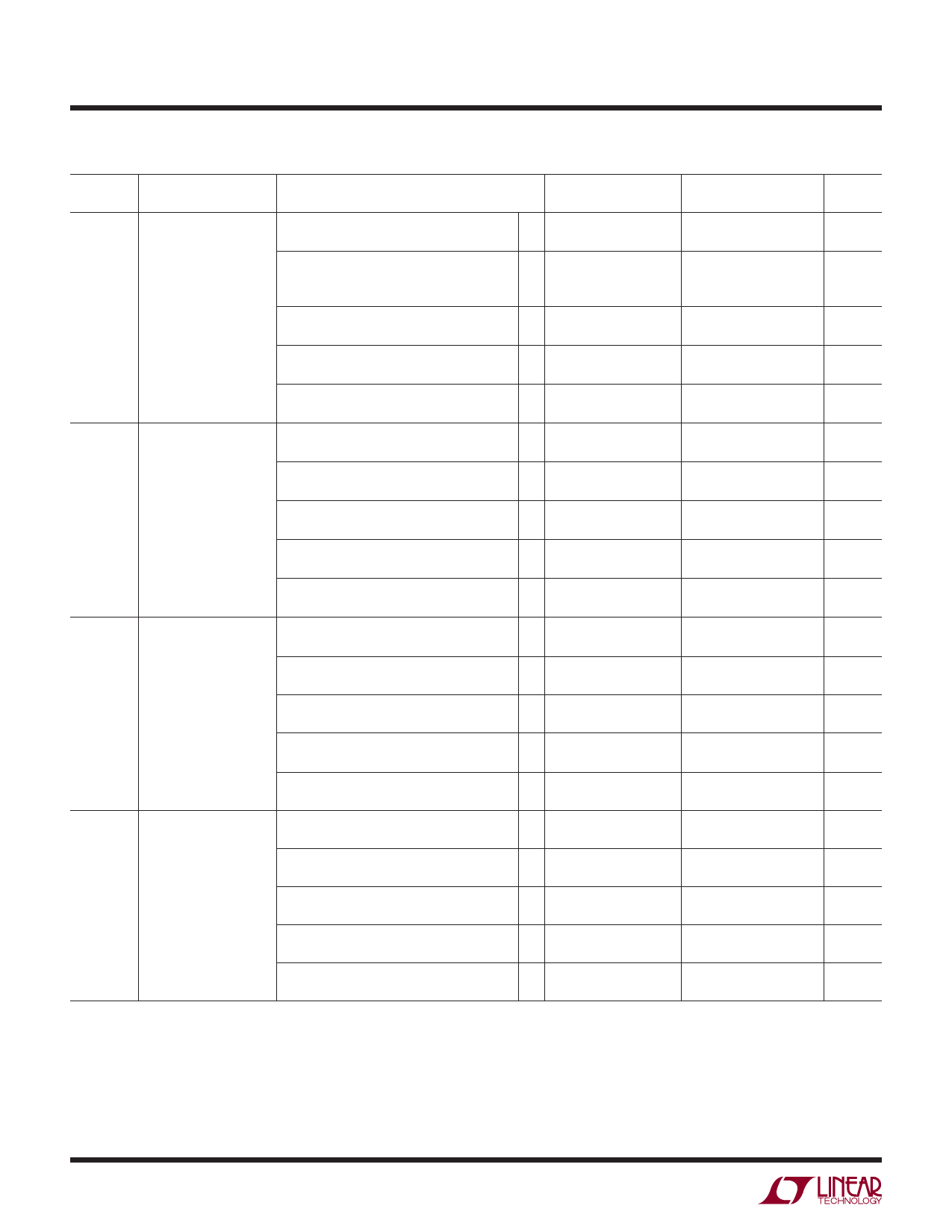
LTC2203/LTC2202
DY A IC ACCURACY The ● denotes the specifications which apply over the full operating temperature range,
otherwise specifications are at TA = 25°C. AIN = –1dBFS unless otherwise noted. (Note 4)
LTC2203
LTC2202
SYMBOL PARAMETER
CONDITIONS
MIN TYP MAX MIN TYP MAX UNITS
S/(N+D) Signal-to-Noise
1MHz Input (2.5V Range, PGA = 0)
81.5
81.5
dBFS
Plus Distortion Ratio 1MHz Input (1.667V Range, PGA = 1)
79.3
79.3
dBFS
5MHz Input (2.5V Range, PGA = 0)
● 79.7 81.5
79.7 81.5
dBFS
5MHz Input (1.667V Range, PGA = 1)
79.3
79.3
dBFS
12.5MHz Input (2.5V Range, PGA = 0)
81.3
12.5MHz Input (1.667V Range, PGA = 1)
79.2
81.3
dBFS
79.2
dBFS
30MHz Input (2.5V Range, PGA = 0)
80.6
80.6
dBFS
30MHz Input (1.667V Range, PGA = 1)
● 77.2 78.6
77.2 78.6
dBFS
70MHz Input (2.5V Range, PGA = 0)
78.1
70MHz Input (1.667V Range, PGA = 1)
77
78.1
dBFS
77
dBFS
SFDR
Spurious Free
1MHz Input (2.5V Range, PGA = 0)
105
105
dBFS
Dynamic Range
1MHz Input (1.667V Range, PGA = 1)
105
105
dBFS
at –25dBFS
5MHz Input (2.5V Range, PGA = 0)
105
105
dBFS
Dither “OFF”
5MHz Input (1.667V Range, PGA = 1)
105
105
dBFS
12.5MHz Input (2.5V Range, PGA = 0)
105
12.5MHz Input (1.667V Range, PGA = 1)
105
105
dBFS
105
dBFS
30MHz Input (2.5V Range, PGA = 0)
105
30MHz Input (1.667V Range, PGA = 1)
105
105
dBFS
105
dBFS
70MHz Input (2.5V Range, PGA = 0)
100
70MHz Input (1.667V Range, PGA = 1)
100
100
dBFS
100
dBFS
SFDR
Spurious Free
1MHz Input (2.5V Range, PGA = 0)
115
115
dBFS
Dynamic Range
1MHz Input (1.667V Range, PGA = 1)
115
115
dBFS
at –25dBFS
5MHz Input (2.5V Range, PGA = 0)
● 100 115
100 115
dBFS
Dither “ON”
5MHz Input (1.667V Range, PGA = 1)
115
115
dBFS
12.5MHz Input (2.5V Range, PGA = 0)
115
12.5MHz Input (1.667V Range, PGA = 1)
115
115
dBFS
115
dBFS
30MHz Input (2.5V Range, PGA = 0)
115
30MHz Input (1.667V Range, PGA = 1)
115
115
dBFS
115
dBFS
70MHz Input (2.5V Range, PGA = 0)
110
70MHz Input (1.667V Range, PGA = 1)
110
110
dBFS
110
dBFS
CO
O
ODE BIAS CHARACTERISTICS The ● denotes the specifications which apply over
the full operating temperature range, otherwise specifications are at TA = 25°C. (Note 4)
PARAMETER
VCM Output Voltage
VCM Output Tempco
VCM Line Regulation
VCM Output Resistance
CONDITIONS
IOUT = 0
IOUT = 0
3.135V ≤ VDD ≤ 3.465V
1mA ≤ | IOUT | ≤ 1mA
MIN TYP MAX UNITS
1.15 1.25 1.35
V
±40
ppm/°C
1
mV/ V
2
Ω
22032fb
4
Share Link: 