M37516E6HP Ver la hoja de datos (PDF) - Renesas Electronics
Número de pieza
componentes Descripción
Lista de partido
M37516E6HP Datasheet PDF : 90 Pages
| |||
7516 Group
[I2C Data Shift Register (S0)] 002B16
The I2C data shift register (S0 : address 002B16) is an 8-bit shift
register to store receive data and write transmit data.
When transmit data is written into this register, it is transferred to
the outside from bit 7 in synchronization with the SCL clock, and
each time one-bit data is output, the data of this register are
shifted by one bit to the left. When data is received, it is input to
this register from bit 0 in synchronization with the SCL clock, and
each time one-bit data is input, the data of this register are shifted
by one bit to the left. The minimum 2 machine cycles are required
from the rising of the SCL clock until input to this register.
The I2C data shift register is in a write enable status only when the
I2C-BUS interface enable bit (ES0 bit : bit 3 of address 002E16) of
the I2C control register is “1”. The bit counter is reset by a write in-
struction to the I2C data shift register. When both the ES0 bit and
the MST bit of the I2C status register (address 002D16) are “1,” the
SCL is output by a write instruction to the I2C data shift register.
Reading data from the I2C data shift register is always enabled re-
gardless of the ES0 bit value.
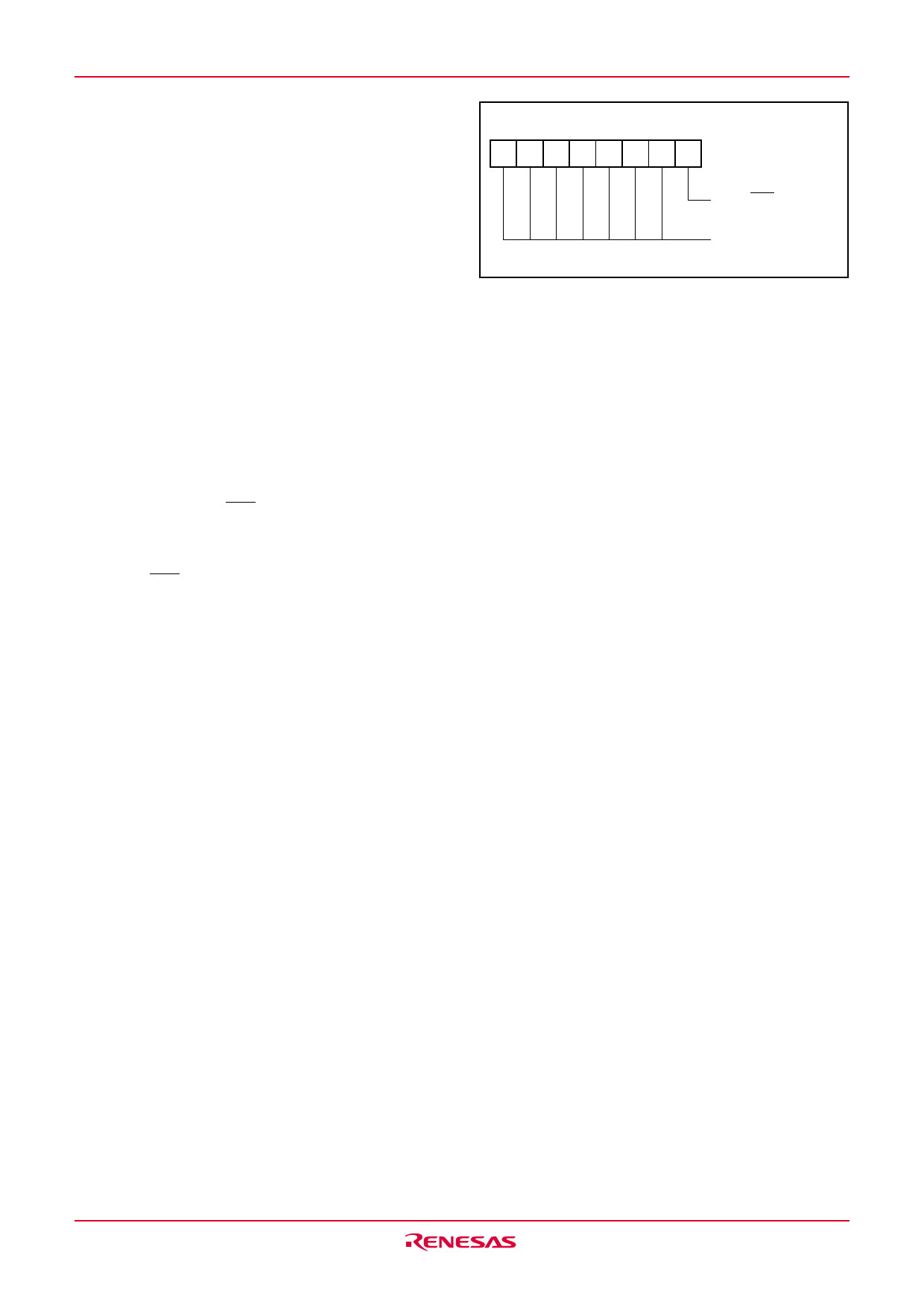
[I2C Address Register (S0D)] 002C16
The I2C address register (address 002C16) consists of a 7-bit
slave address and a read/write bit. In the addressing mode, the
slave address written in this register is compared with the address
data to be received immediately after the START condition is de-
tected.
•Bit 0: Read/write bit (RWB)
This is not used in the 7-bit addressing mode. In the 10-bit ad-
dressing mode, the first address data to be received is compared
with the contents (SAD6 to SAD0 + RWB) of the I2C address reg-
ister.
The RWB bit is cleared to “0” automatically when the stop condi-
tion is detected.
•Bits 1 to 7: Slave address (SAD0–SAD6)
These bits store slave addresses. Regardless of the 7-bit address-
ing mode and the 10-bit addressing mode, the address data
transmitted from the master is compared with the contents of
these bits.
b7
b0
SAD6 SAD5 SAD4 SAD3 SAD2 SAD1 SAD0 RWB
I2C address register
(S0D: address 002C16)
Read/write bit
Slave address
Fig. 28 Structure of I2C address register
Rev.1.01 Jul 01, 2003 page 30 of 89
Share Link: 