MAX2383 Ver la hoja de datos (PDF) - Maxim Integrated
Número de pieza
componentes Descripción
Lista de partido
MAX2383 Datasheet PDF : 8 Pages
| |||
W-CDMA Upconverter and PA Driver
with Power Control
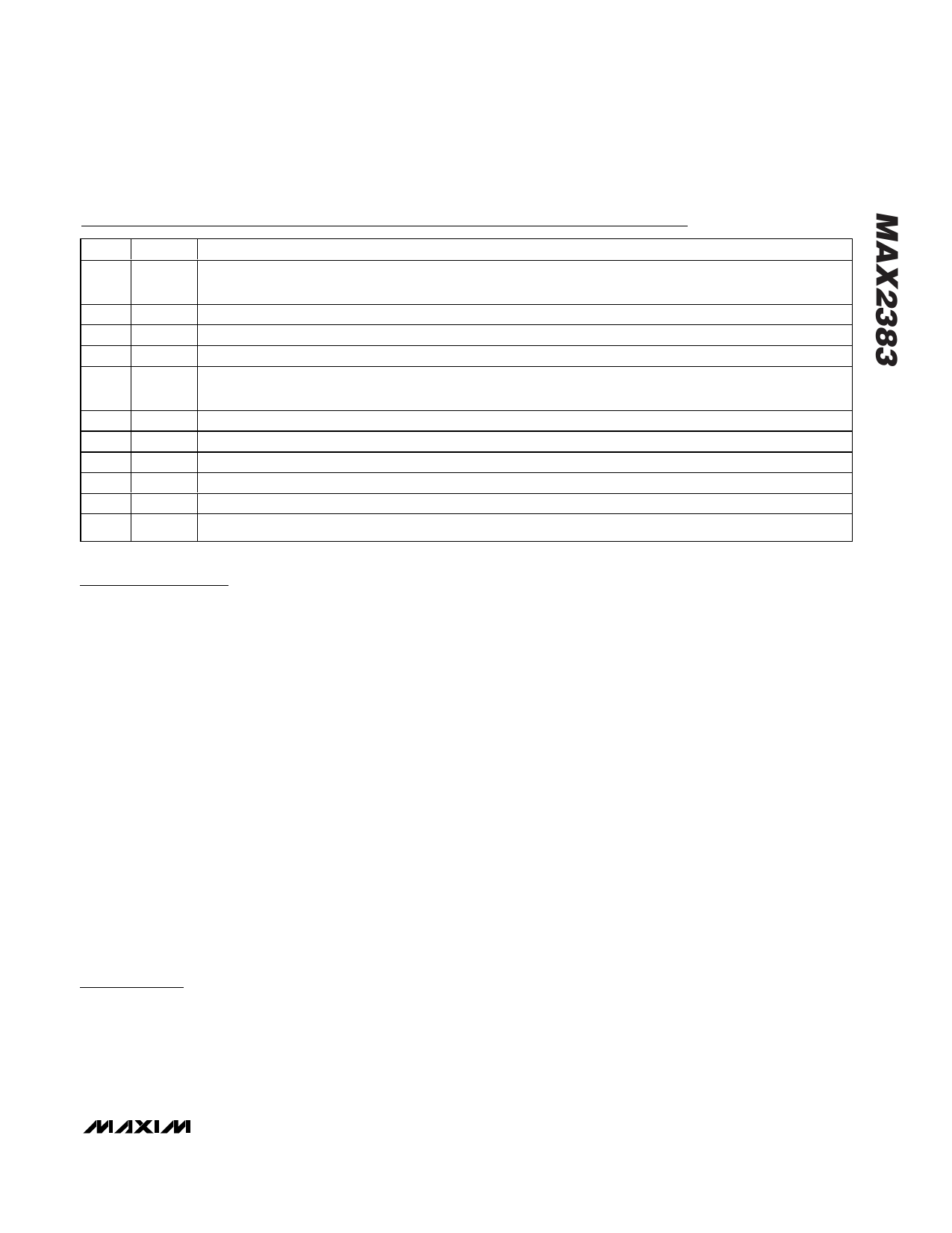
Pin Description
PIN NAME
FUNCTION
A1+
LO_EN
/LO+
LO Buffer Enable Pin. When LOW, the LO buffer shuts off. Also noninverting input for LO port. It can be AC-
coupled to GND, when the LO is driven single-ended.
A2
VCC Power-Supply Pin. Bypass with a 330pF capacitor to GND as close to the pin as possible.
A3 DROUT PA Driver Output Pin. Externally matched to 50Ω.
A4
GND Ground Reference for RF
B1
SHDN/ Shutdown Pin. When LOW, the entire part shuts off, except for LO buffer. Also inverting input for LO port. It
LO- can be AC-coupled to GND, when the LO is driven single-ended.
B3
GC
Power Control Input Pin (0.5V to 2.0V for control voltage)
B4
DRIN PA Driver Input Pin (interstage node). Can be externally matched to 50Ω.
C1
IFIN- Inverting IF Input (400Ω differential nominal impedance between IFIN+ and IFIN-)
C2
IFIN+ Noninverting IF Input (400Ω differential nominal impedance between IFIN+ and IFIN-)
C3 RFOUT Upconverter Output Port (interstage node). Can be externally matched to 50Ω.
C4
GND Ground Reference for RF
Detailed Description
Variable-Gain Mixer
The MAX2383 contains a double-balanced Gilbert cell
mixer merged with a gain-control circuit, followed by a
mixer buffer. The mixer is driven differentially at its IF
ports. The LO input for the mixer is conditioned through
a low-noise, inductively loaded buffer. The mixer differ-
ential output is driven through an on-chip balun into a
single-ended common emitter amplifier, which drives
the output pin (RFOUT). The mixer buffer is a single-
ended in/out common emitter stage with inductive
degeneration and an external inductive load.
Additionally, these circuits are biased from “VCS” gen-
erators, designed to produce a low-noise constant
degeneration voltage at the user’s current source.
These bias circuits also provide the control required to
selectively power-down the circuit and also provide for
gain control and current throttle-back.
PA Driver
The PA buffer is a single-ended in/out common emitter
stage with inductive degeneration and an external
inductive load.
Applications Information
LO Buffer Inputs
The external LO is interfaced either differentially or sin-
gle-ended to the differential LO buffer. Those two pins
also function as the control inputs for the device.
Hence, they are DC-coupled to the chip-control circuit-
ry, and AC-coupled to the LO port. SHDN and LO_EN
turn off the whole IC when both pins are pulled LOW.
LO_EN helps reduce VCO pulling in gated-transmission
mode by providing means to keep the LO buffer on
while the upconverter and driver turn on and off. To
avoid loading of the LO buffer, connect a 10kΩ isolation
resistor between the LO_EN/LO+ pin and the LO_EN
logic input, and a 10kΩ isolation resistor between the
SHDN/LO- pin and the SHDN logic input.
Differential IF Inputs
The MAX2383 has a differential IF input port for inter-
facing to differential IF filters. The IF pins should be AC-
coupled to the IF ports. The typical IF frequency is
380MHz, but the device can operate from 200MHz to
600MHz. The differential impedance between the two IF
inputs is approximately 400Ω in parallel with 1.0pF.
Interstage Matching
The mixer buffer drives the following PA driver through
an interstage matching network connected between the
mixer’s RFOUT pin and the PA driver’s input pin (DRIN).
This off-chip matching network, which consists of two
series inductors and a parallel capacitor, is designed to
achieve better than 25dBc image suppression with no
current consumption penalty. The quality factor of this
off-chip resonant circuit determines the image suppres-
sion level and usable bandwidth from the point of view
of passband gain flatness.
PA Driver Output
The PA driver output, DROUT, is an open-collector out-
put that requires an external inductor to VCC for proper
biasing. The output matching components are chosen
_______________________________________________________________________________________ 5
Share Link: 