MC100EP105(2002) Ver la hoja de datos (PDF) - ON Semiconductor
Número de pieza
componentes Descripción
Lista de partido
MC100EP105 Datasheet PDF : 8 Pages
| |||
MC10EP105, MC100EP105
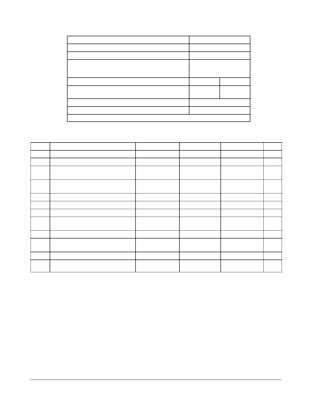
MAXIMUM RATINGS (Note 2)
Symbol
Parameter
Condition 1
VCC
PECL Mode Power Supply
VEE
NECL Mode Power Supply
VI
PECL Mode Input Voltage
NECL Mode Input Voltage
Iout
Output Current
VEE = 0 V
VCC = 0 V
VEE = 0 V
VCC = 0 V
Continuous
Surge
IBB
VBB Sink/Source
TA
Operating Temperature Range
Tstg
Storage Temperature Range
θJA
Thermal Resistance (Junction–to–Ambient) 0 LFPM
500 LFPM
θJC
Thermal Resistance (Junction–to–Case)
std bd
Tsol
Wave Solder
< 2 to 3 sec @ 248°C
2. Maximum Ratings are those values beyond which device damage may occur.
Condition 2
VI ≤ VCC
VI ≥ VEE
32 LQFP
32 LQFP
32 LQFP
Rating
6
–6
6
–6
50
100
± 0.5
–40 to +85
–65 to +150
80
55
12 to 17
265
Units
V
V
V
V
mA
mA
mA
°C
°C
°C/W
°C/W
°C/W
°C
10EP DC CHARACTERISTICS, PECL VCC = 3.3 V, VEE = 0 V (Note 3)
–40°C
25°C
85°C
Symbol
Characteristic
Min Typ Max Min Typ Max Min Typ Max Unit
IEE
VOH
VOL
VIH
VIL
VIHCMR
Power Supply Current
Output HIGH Voltage (Note 4)
Output LOW Voltage (Note 4)
Input HIGH Voltage (Single–Ended)
Input LOW Voltage (Single–Ended)
Input HIGH Voltage Common Mode
Range (Differential) (Note 5)
45
58
75
45
59
75
45
60
75 mA
2165 2290 2415 2230 2355 2480 2290 2415 2540 mV
1365 1490 1615 1430 1555 1680 1490 1615 1740 mV
2090
2415 2155
2480 2215
2540 mV
1365
1690 1460
1755 1490
1815 mV
2.0
3.3 2.0
3.3 2.0
3.3
V
IIH
Input HIGH Current
150
150
150 µA
IIL
Input LOW Current
0.5
0.5
0.5
µA
NOTE: EP circuits are designed to meet the DC specifications shown in the above table after thermal equilibrium has been established. The
circuit is in a test socket or mounted on a printed circuit board and transverse airflow greater than 500 lfpm is maintained.
3. Input and output parameters vary 1:1 with VCC. VEE can vary +0.3 V to –2.2 V.
4. All loading with 50 Ω to VCC–2.0 volts.
5. VIHCMR min varies 1:1 with VEE, VIHCMR max varies 1:1 with VCC. The VIHCMR range is referenced to the most positive side of the differential
input signal.
10EP DC CHARACTERISTICS, PECL VCC = 5.0 V, VEE = 0 V (Note 6)
–40°C
25°C
85°C
Symbol
Characteristic
Min Typ Max Min Typ Max Min Typ Max Unit
IEE
VOH
VOL
VIH
VIL
VIHCMR
Power Supply Current
Output HIGH Voltage (Note 7)
Output LOW Voltage (Note 7)
Input HIGH Voltage (Single–Ended)
Input LOW Voltage (Single–Ended)
Input HIGH Voltage Common Mode
Range (Differential) (Note 8)
45
58
75
45
59
75
45
60
75 mA
3865 3990 4115 3930 4055 4180 3990 4115 4240 mV
3065 3190 3315 3130 3255 3380 3190 3315 3440 mV
3790
4115 3855
4180 3915
4240 mV
3065
3390 3130
3455 3190
3515 mV
2.0
5.0 2.0
5.0 2.0
5.0
V
IIH
Input HIGH Current
150
150
150 µA
IIL
Input LOW Current
0.5
0.5
0.5
µA
NOTE: EP circuits are designed to meet the DC specifications shown in the above table after thermal equilibrium has been established. The
circuit is in a test socket or mounted on a printed circuit board and transverse airflow greater than 500 lfpm is maintained.
6. Input and output parameters vary 1:1 with VCC. VEE can vary +2.0 V to –0.5 V.
7. All loading with 50 Ω to VCC–2.0 volts.
8. VIHCMR min varies 1:1 with VEE, VIHCMR max varies 1:1 with VCC. The VIHCMR range is referenced to the most positive side of the differential
input signal.
http://onsemi.com
3
Share Link: 