MC145532 Ver la hoja de datos (PDF) - Motorola => Freescale
Número de pieza
componentes Descripción
Lista de partido
MC145532 Datasheet PDF : 16 Pages
| |||
DECODER OUTPUT — SHORT FRAME
Figure 7 shows the timing of the decoder output in short
frame mode.
The DDO will provide the 8–bit PCM word for the decoding
rate that was selected for this frame of data on the decoder
input pins. The data is loaded into the MC145532 during one
frame, decoded on the next frame, and read during the third
frame.
DECODER OUTPUT — LONG FRAME
Figure 8 shows the timing of the decoder output in long
frame mode. Note that at least eight bits are presented to the
output, provided that at least two falling edges of DDC are
seen while DOE is high. The enable can be used to extend
the LSB to a full DDC period and/or cause the eight bits of
data to be recirculated to the output pin until the enable falls.
STANDARDS INFORMATION
The following standards apply to the MC145532:
T1.301–1987 — 32 kbps ADPCM
T1.303–1988 — 24 kbps ADPCM
CCITT G.721–1988, G.723–1988, and G.726 — 32 kbps
and 24 kbps
CCITT, ITU–T, TIA, and EIA documents may be obtained
by contacting Global Engineering Documents in the USA at
(800) 854–7179, or internationally at (303) 397–7956.
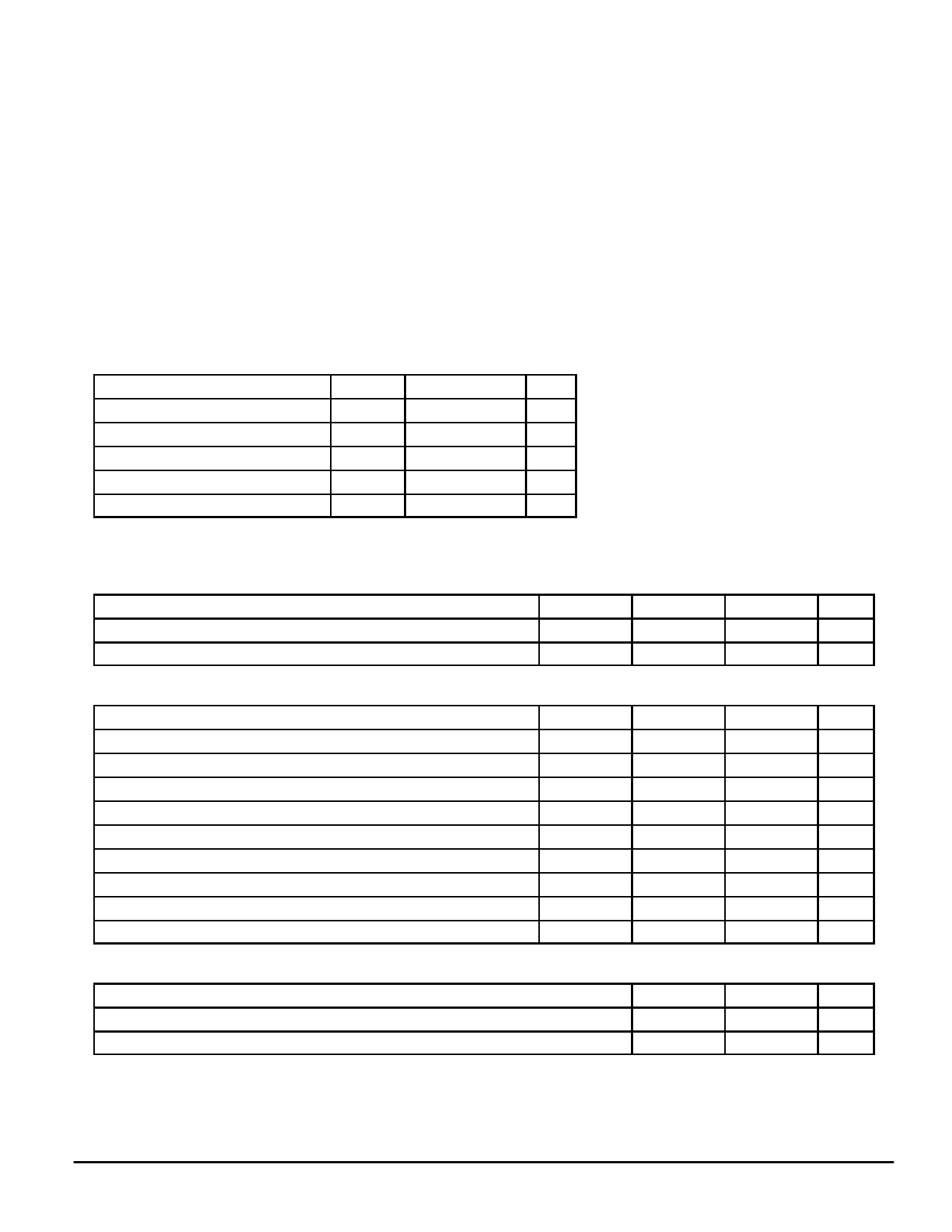
ABSOLUTE MAXIMUM RATINGS (Voltages Referenced to VSS)
Rating
Symbol
Value
DC Supply Voltage
Voltage, Any Pin to VSS
DC Current, Any Pin
Operating Temperature
Storage Temperature
VDD
V
Iin
TA
Tstg
– 0.5 to + 7.0
– 0.5 to VDD + 0.5
± 10
– 40 to + 85
– 85 to + 150
RECOMMENDED OPERATING CONDITIONS (TA = – 40 to + 85°C)
Parameter
DC Supply Voltage
Power Dissipation
Unit
This device contains circuitry to protect
against damage due to high static voltages or
V
electric fields; however, it is advised that
V
normal precautions be taken to avoid appli-
cation of any voltage higher than maximum
mA
rated voltages to this high impedance circuit.
°C
For proper operation it is recommended that
Vin and Vout be constrained to the range VSS ≤
°C
(Vin or Vout) ≤ VDD.
Unused inputs must always be tied to an
appropriate logic voltage level (e.g., either VSS
or VDD).
Symbol
Min
VDD
4.50
PD
—
Max
Unit
5.50
V
0.28
W
DIGITAL CHARACTERISTICS (VDD = 5.0 V, TA = – 40 to + 85°C)
Parameter
High Level Input Voltage Mode, DOE, DDC, DDI, DIE, EIE, EDI, EDC, EOE
Low Level Input Voltage Mode, DOE, DDC, DDI, DIE, EIE, EDI, EDC, EOE
High Level Input Voltage
RESET, APD, SPC
Low Level Input Voltage
RESET, APD, SPC
Input Current
Input Capacitance
High Level Output Voltage (IOH = – 2.0 mA)
Low Level Output Voltage (IOL = 2.0 MA)
Output Leakage Current (VDD = 5.5 V)
DDO, EDO
DDO, EDO
DDO, EDO
Symbol
VIH
VIL
VIH
VIL
Iin
Cin
VOH
VOL
Ilkg
Min
2.0
—
0.7 VDD
—
—
—
4.6
—
—
Max
Unit
—
V
0.8
V
—
V
0.3 VDD
V
± 1.0
µA
10
pF
—
V
0.4
V
± 5.0
µA
SWITCHING CHARACTERISTICS (VDD = 5.0 V, TA = – 40 to + 85°C)
Parameter
SPC Frequency
SPC Duty Cycle
Min
19.990
45
Max
Unit
23
MHz
55
%
MC145532
4
MOTOROLA
Share Link: 