MEJ02C2016_M5M5J167KT Ver la hoja de datos (PDF) - Hitachi -> Renesas Electronics
Número de pieza
componentes Descripción
Lista de partido
MEJ02C2016_M5M5J167KT
Hitachi -> Renesas Electronics

MEJ02C2016_M5M5J167KT Datasheet PDF : 11 Pages
| |||
Jan.10,2003 Ver. 2.1
M5M5J167KT - 70HI
MITSUBISHI LSIs
16777216-BIT (1048576-WORD BY 16-BIT / 2097152-WORD BY 8-BIT) CMOS STATIC RAM
POWER DOWN CHARACTERISTICS
(1) ELECTRICAL CHARACTERISTICS (Ta=-40~85ºC, Vcc=2.7V~3.6V,unless otherwise noted)
Symbol
Parameter
Vcc (PD) Power down supply voltage
VI (BC)
Byte control input
BC1# & BC2#
Test conditions
Limits
Min
Ty p Max
2.0
2.0
Units
V
V
VI (S1#) Chip select input S1#
2.0
V
VI (S2) Chip select input S2
0.2
Icc (PD) Power down
supply c urrent
Vcc=2.0V
(1) S1# > Vcc - 0.2V, BYTE# > Vcc - 0.2V or < 0.2V
other inputs = 0 ~ Vcc
(2) S2 < 0.2V , BYTE# > Vcc - 0.2V or < 0.2V
other inputs = 0 ~ Vcc
(3) BC1# and BC2# > Vcc - 0.2V
S1# < 0.2V, S2 > Vcc - 0.2V
BYTE# > Vcc - 0.2V or < 0.2V
other inputs = 0 ~ Vcc
~ +25°C
~ +40°C
~ +70°C
~ +85°C
-
0.2 3.0
-
0.4 6.0
µA
-
-
30
-
-
60
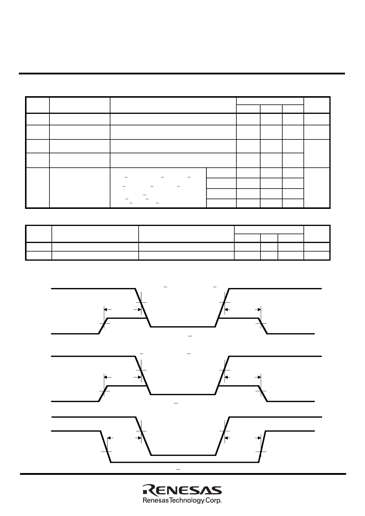
(2) TIMING REQUIREMENTS
Note 9: Typical parameter of Icc(PD) indicates the value for the
center of distribution at 2.0V, and not 100% tested.
Symbol
Parameter
tsu (PD)
trec (PD)
Power down set up time
Power down recov ery t ime
Test conditions
Limits
Min Ty p Max
0
5
Units
ns
ms
(3) TIMING DIAGRAM
BC# control mode
Vcc
note10:On the BC# control mode, the lev el of S1# and S2 must be f ixed
at S1#, S2, A19 > Vcc-0.2V or S2 <0.2V
tsu (PD)
2.7V
2.7V
trec (PD)
BC1#
BC2#
2.2V
S1# control mode
Vcc
2.2V
BC1# , BC2# > Vcc - 0.2V
note11:On the S1# control mode, the lev el of S2 must be f ixed
at S2 > Vcc-0.2V or S2 <0.2V
tsu (PD)
2.7V
2.7V
trec (PD)
2.2V
S1#
S2 control mode
Vcc
S1# > Vcc - 0.2V
2.2V
S2
2.7V
2.7V
tsu (PD)
trec (PD)
0.2V
0.2V
S2 < 0.2V
9
Share Link: