MK2049-02 Ver la hoja de datos (PDF) - Integrated Circuit Systems
Número de pieza
componentes Descripción
Lista de partido
MK2049-02 Datasheet PDF : 12 Pages
| |||
MK2049-02/03
Communications Clock PLLs
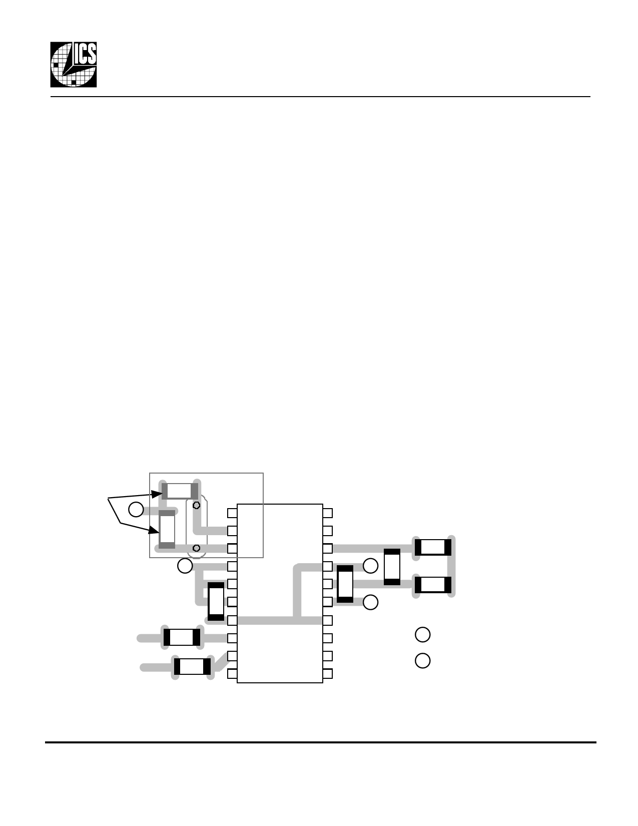
LAYOUT AND EXTERNAL COMPONENTS
The MK2049-02/03 require a minimum number of external components for proper operation. Decoupling
capacitors of 0.01µF must be connected between VDD and GND pins close to the chip (especially pins 4
and 7, 15 and 17), and 33 Ω terminating resistors should be used on clock outputs with traces longer than 1
inch (assuming 50 Ω traces).
PC Board Layout
A proper board layout is critical to the successful use of the MK2049. In particular, the CAP1 and CAP2 pins
are very sensitive to noise and leakage (CAP2 at pin 18 is the most sensitive). Traces must be as short as
possible and the two capacitors and resistor must be mounted next to the device as shown below. The
capacitor shown between pins 15 and 17, and the one between pins 5 and 7 are the power supply decoupling
capacitors. The high frequency output clocks on pins 8 and 9 should have a series termination of 33 Ω
connected close to the pin. Additional improvements will come from keeping all components on the same
side of the board, minimizing vias through other signal layers, and routing other signals away from the
MK2049. You may also refer to MAN05 for additional suggestions on layout of the crystal section.
The crystal traces should include pads for small capacitors from X1 and X2 to ground; these are used to
adjust the stray capacitance of the board to match the crystal load capacitance. The typical telecom reference
frequency is accurate to much less than 1 ppm, so the MK2049 may lock and run properly even if the board
capacitance is not adjusted with these fixed capacitors. However, ICS MicroClock recommends that the
adjustment capacitors be included to minimize the effects of variation in individual crystals, temperature,
and aging. The value of these capacitors (typically 0-4 pF) is determined once for a given board layout,
using the procedure described in the section titled “Determining the Crystal Frequency Adjustment
Capacitors”.
Cutout in ground and power plane.
cap
Optional;
Route all traces away from this area.
see text G
1
20
cap
2
19
3
18
resist.
V
4
17
G cap
5
16 cap
cap
cap 6
15
V
7
14
resist.
8
13
V =connect to VDD
9
12
resist.
10
11
G =connect to GND
Figure 3. Typical MK2049-02/03 Layout
MDS 2049-02/03 B
8
Revision 040601
Integrated Circuit Systems, Inc. • 525 Race Street • San Jose • CA • 95126 • (408)295-9800tel• www.icst.com
Share Link: 