ML7022-01 Ver la hoja de datos (PDF) - Oki Electric Industry
Número de pieza
componentes Descripción
Lista de partido
ML7022-01 Datasheet PDF : 20 Pages
| |||
1Semiconductor
FEDL7022-01-06
ML7022-01
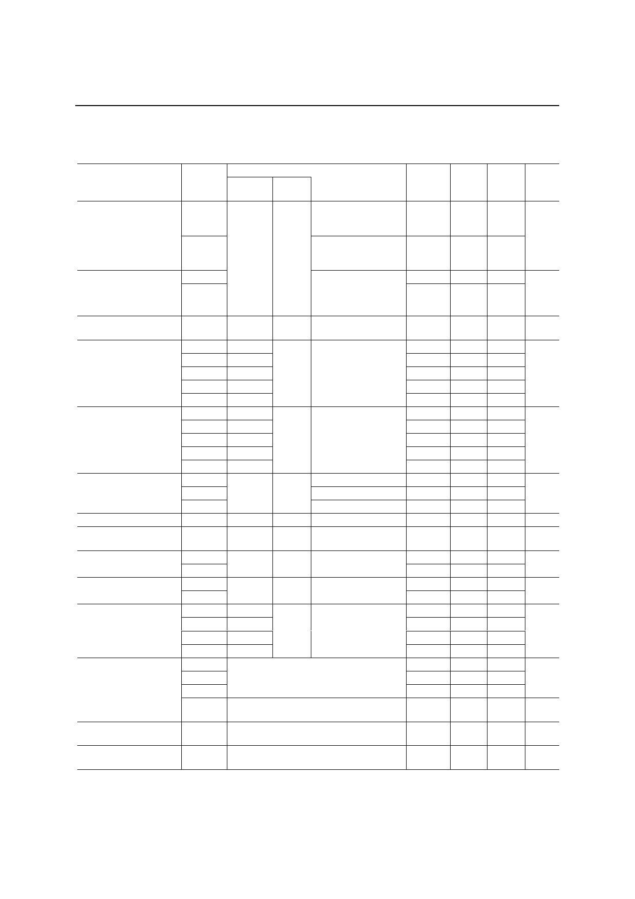
AC Characteristics (Continued)
Condition
(VDD = 4.75 to 5.25 V, Ta = –40 to +85°C)
Parameter
Symbol Freq. Level
(Hz) (dBm0)
Min. Typ. Max. Unit
Absolute Level
(Initial Difference)
AVT
AVR
1020
0
GSXn to DOUT
VDD = 5 V,
Ta = 25°C
DIN to AOUTn
VDD = 5 V,
Ta = 25°C
0.535
0.806
0.555
0.835
0.574
0.864
Vrms
Absolute level
(Deviation of
Temperature and
power)
AVTT
AVRT
–0.3
—
0.3
VDD = 4.75 to 5.25 V
Ta = –40 to 85°C –0.3
—
dB
0.3
Absolute Delay
TD
1020
0
A to A Mode
BCLK = 2048 kHz
—
0.58 0.6 ms
TGD T1
500
—
TGD T2
600
—
Transmit Group Delay TGD T3 1000
0
*3
—
TGD T4 2600
—
TGD T5 2800
—
TGD R1
500
—
TGD R2
600
—
Receive Group Delay TGD R3 1000
0
*3
—
TGD R4 2600
—
TGD R5 2800
—
Cross Talk
Attenuation
CRT
CRR
CRCH
1020
Trans to Receive
75
0
Receive to Trans
75
Channel to Channel 75
Discrimination
DIS 4.6 to 72k 0
0 to 4 kHz
30
0.26 0.75
0.16 0.35
0.02 0.125 ms
0.05 0.125
0.07 0.75
0.00 0.75
0.00 0.35
0.00 0.125 ms
0.09 0.125
0.12 0.75
83
—
80
—
dB
78
—
32
—
dB
Out of Band Spurious
OBS
300 to
3.4k
0 4.6 kHz to 1000 kHz — –37.5 –35 dB
Signal Frequency
Distortion
SFDT
1020
0
SFDR
0 to 4 kHz
—
–50 –40
dBm0
—
–48 –40
Intermoduration
Distortion
IMDT fa = 470 –4
IMDR fb = 320
2 fa - fb
—
–50 –40
dBm0
—
–54 –40
PSRT1 0 to 4k
40
44
—
Power Supply Noise
PSRT2 4 to 50k 100
*4
Rejection Ratio
PSRR1 0 to 4k mVrms
50
55
—
dB
40
45
—
PSRR2 4 to 50k
50
56
—
TSD
DOUT
20
— 100
Digital Output
Delay Time
TXD1
TXD2
TPDC
Pull-up resister = 0.5 kΩ
CL = 50 pF and 1 LSTTL
C1A, C2A, C3A, C1B, C2B, C3B
CL = 50 pF and 1 LSTTL
20
— 100 ns
20
— 100
20
— 1000 ns
DOUT Operation
Delay Time
TDDO Time of operation start after power on
—
4
—
ms
AOUT Signal Output
Delay Time
TDAO
Time of base band signal output start
after power on
—
4
—
ms
*3 Minimum value of the group delay distortion
*4 The measurement under idle channel noise
8/20
Share Link: 