FEDR27V3252J-01-02 Ver la hoja de datos (PDF) - Oki Electric Industry
Número de pieza
componentes Descripción
Lista de partido
FEDR27V3252J-01-02 Datasheet PDF : 12 Pages
| |||
OKI Semiconductor
FEDR27V3252J-01-02
MR27V3252J / OTP
ELECTRICAL CHARACTERISTICS
DC Characteristics
Parameter
Input leakage current
Output leakage current
VCC power supply current
(Standby)
VCC power supply current
(Read)
VPP power supply current
Input “H” level
Input “L” level
Output “H” level
Output “L” level
Symbol
ILI
ILO
ICCSC
ICCST
ICCA1
IPP
VIH
VIL
VOH
VOL
Condition
VI = 0 to VCC
VO = 0 to VCC
CE# = VCC
CE# = VIH
OE# = VIH, f = 10MHz
VPP = VCC
—
—
IOH = –1 mA
IOL = 2 mA
(VCC = 3.0 V to 3.6 V, Ta = 0 to 70°C)
Min.
Typ.
Max.
Unit
—
—
5
µA
—
—
5
µA
—
—
10
µA
—
—
1
mA
—
—
50
mA
—
2.2
–0.5∗∗
2.4
—
—
10
µA
—
VCC+0.5∗
V
—
0.6
V
—
—
V
—
0.4
V
Voltage is relative to VSS.
∗ : Vcc+1.5V(Max.) when pulse width of overshoot is less than 10ns.
∗∗ : -1.5V(Min.) when pulse width of undershoot is less than 10ns.
AC Characteristics
Parameter
Address cycle time
Address access time
Page cycle time
Page access time
CE# access time
OE# access time
Output disable time
Output hold time
Symbol
tC
tACC
tPC
tPAC
tCE
tOE
tCHZ
tOHZ
tOH
Condition
—
CE# = OE# = VIL
—
—
OE# = VIL
CE# = VIL
OE# = VIL
CE# = VIL
CE# = OE# = VIL
Measurement conditions
Input signal level --------------------------------------0 V/3.0 V
Input timing reference level-------------------------1/2Vcc
Output load ---------------------------------------------50 pF
Output timing reference level ----------------------1/2Vcc
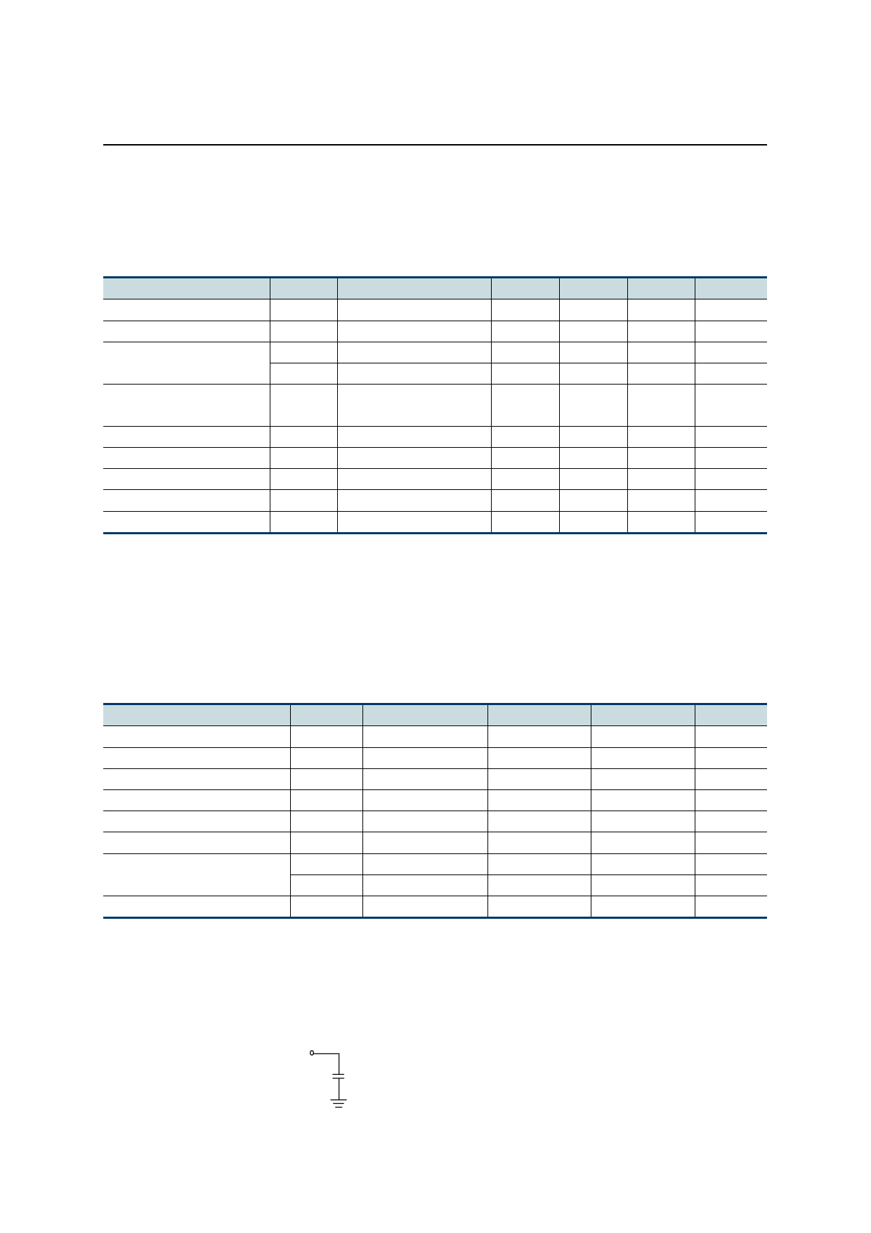
Output load
Output
50 pF
(Including scope and jig)
(VCC = 3.0 V to 3.6 V, Ta = 0 to 70°C)
Min.
Max.
Unit
70
—
ns
—
70
ns
25
—
ns
—
25
ns
—
70
ns
—
25
ns
0
20
ns
0
20
ns
0
—
ns
4/12
Share Link: 