MSM7583 Ver la hoja de datos (PDF) - Oki Electric Industry
Número de pieza
componentes Descripción
Lista de partido
MSM7583 Datasheet PDF : 23 Pages
| |||
¡ Semiconductor
MSM7583
ENV
Quadrature modulation signal envelope ( I2 + Q2 ) output.
Its output level is 500 mVpp with 1.6 Vdc as a center value. The output pin load conditions are:
R ≥ 10 kW , C £ 20 pF. The gain of this output can be adjusted using the control registers CR2
- B7 to B4.
This pin is also used to monitor eye pattern, AFC compensating signal, and phase detection of
the demodulator block during the test mode. Refer to the description of the control register for
details.
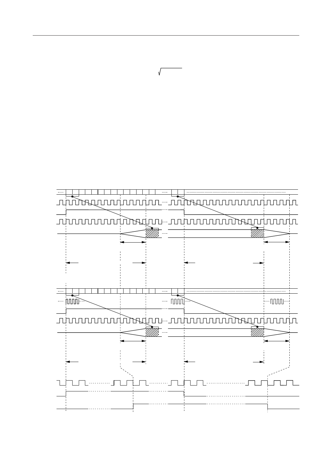
BSTO
Modulation burst window signal output.
The burst position for the I/Q baseband modulation output is output. (Refer to Fig. 1.)
(1) CR0 - B6 ="0".
TXD
TXCI
(384 kHz)
TXW
TXCO
(384 kHz)
I, Q
D0 D1 D2 D3 D4 D5 D6 D7 D8 D9 D10D11D12D13
Dn-1 Dn
Ramp rise-up
2 symbols
Delay of 6.25 symbols
Ramp fall-down
2 symbols
Delay of 6.25 symbols
(2) CR0 - B6 ="1".
TXD
TXCI
(3.84 MHz)
TXW
TXCO
(384 kHz)
I, Q
D0 D1 D2 D3 D4 D5 D6 D7 D8 D9 D10D11D12D13
Dn-1 Dn
Ramp rise-up
2 symbols
Delay of 6.25 symbols
Ramp fall-down
2 symbols
Delay of 6.25 symbols
TXCI
(384 kHz)
TXW
BSTO
12
8 9 10
N
N+1 N+2
Figure 1 Transmitter Timing Diagram
N+16 N+17 N+18 N+19
5/23
Share Link: 