NCV8660B(2010) Ver la hoja de datos (PDF) - ON Semiconductor
Número de pieza
componentes Descripción
Lista de partido
NCV8660B
(Rev.:2010)
(Rev.:2010)
ON Semiconductor

NCV8660B Datasheet PDF : 12 Pages
| |||
NCV8660B
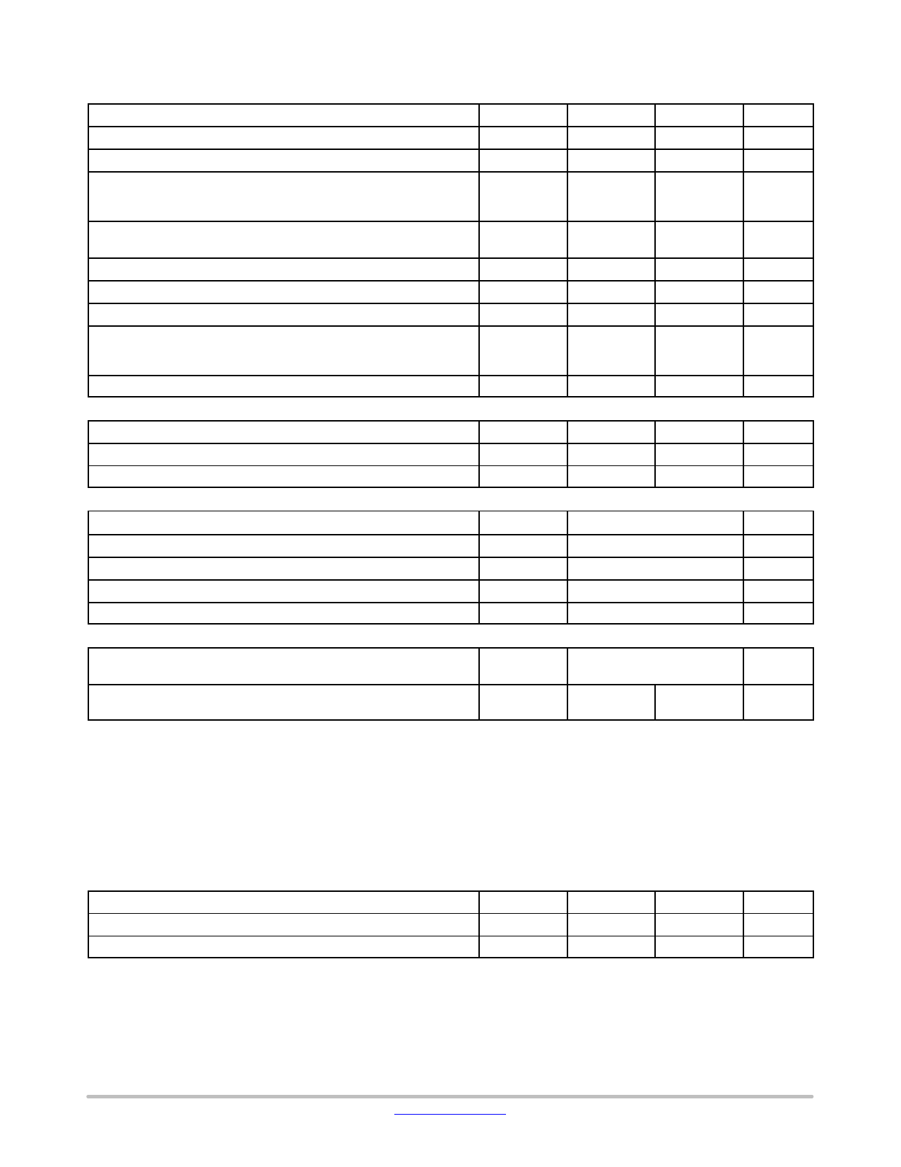
ABSOLUTE MAXIMUM RATINGS
Rating
Symbol
Min
Max
Unit
Input Voltage (IN)
Input Current
Output Voltage (OUT)
DC
Transient, t < 10 s (Note 1)
VIN
IIN
VOUT
−0.3
−1.0
−0.3
−0.3
40
V
−
mA
V
5.5
16
Output Current (OUT)
IOUT
−1.0
Current
mA
Limited
Storage Temperature Range
DT (Reset Delay Time Select) Voltage (Note 2)
DT (Reset Delay Time Select) Current (Note 2)
RO (Reset Output) Voltage
DC
Transient, t < 10 s
TSTG
VDT
IDT
VRO
−55
−0.3
−1.0
−0.3
−0.3
150
°C
16
V
1.0
mA
V
5.5
16
RO (Reset Output) Current
ESD CAPABILITY
IRO
−1.0
1.0
mA
ESD Capability, Human Body Model (Note 3)
ESD Capability, Machine Model (Note 3)
ESD Capability, Charged Device Model (Note 3)
THERMAL RESISTANCE
ESDHB
ESDMM
ESDCDM
−2.0
−200
−1.0
2.0
kV
200
V
1.0
kV
Junction−to−Ambient (Note 4)
Junction−to−Lead (pin 6) (Note 4)
LEAD SOLDERING TEMPERATURE AND MSL
RqJA
RqJT
104
°C/W
33
°C/W
Moisture Sensitivity Level
MSL
3
−
Lead Temperature Soldering: SMD style only, Reflow (Note 5)
Pb−Free Part 60 − 150 sec above 217°C, 40 sec max at peak
SLD
−
265 peak
°C
Stresses exceeding Maximum Ratings may damage the device. Maximum Ratings are stress ratings only. Functional operation above the
Recommended Operating Conditions is not implied. Extended exposure to stresses above the Recommended Operating Conditions may affect
device reliability.
1. The output voltage must not exceed the input voltage.
2. External resistor required to minimize current to less than 1 mA when the control voltage is above 16 V.
3. This device series incorporates ESD protection and is tested by the following methods:
ESD HBM tested per AEC−Q100−002 (EIA/JESD22−A114)
ESD MM tested per AEC−Q100−003 (EIA/JESD22−A115)
ESD CDM tested per EIA/JESD22/C101, Field Induced Charge Model
4. Values represented typical steady−state thermal performance on 1 oz. copper FR4 PCB with 1 in2 copper area.
5. Per IPC / JEDEC J−STD−020C.
OPERATING RANGE
Pin Symbol, Parameter
VIN, Input Voltage Operating Range
Junction Temperature Range
Symbol
Min
VIN
4.5
TJ
−40
Max
Unit
40
V
150
°C
http://onsemi.com
3
Share Link: