P172 Ver la hoja de datos (PDF) - Agere -> LSI Corporation
Número de pieza
componentes Descripción
Lista de partido
P172 Datasheet PDF : 8 Pages
| |||
P172-Type Receiver
Advance Data Sheet
August 2001
Description
The P172-type receiver consists of a PIN or APD cou-
pled to a single-mode or multimode fiber pigtail and a
linear preamplifier. Both the PIN and APD are rear-illu-
minated planar diode structures with a low-capacitance
active area for maximum responsivity and speed.
This device incorporates the new Laser 2000 manufac-
turing process from the Optoelectronics Products unit
of Agere Systems Inc. Laser 2000 is a low-cost plat-
form that targets high-volume manufacturing and tight
product distributions on all optical subassemblies. This
platform incorporates an advanced optical design that
is produced on Agere Systems’ highly automated pro-
duction lines. The Laser 2000 platform is qualified for
central office and uncontrolled environments, and can
be used for applications requiring high performance
and low cost.
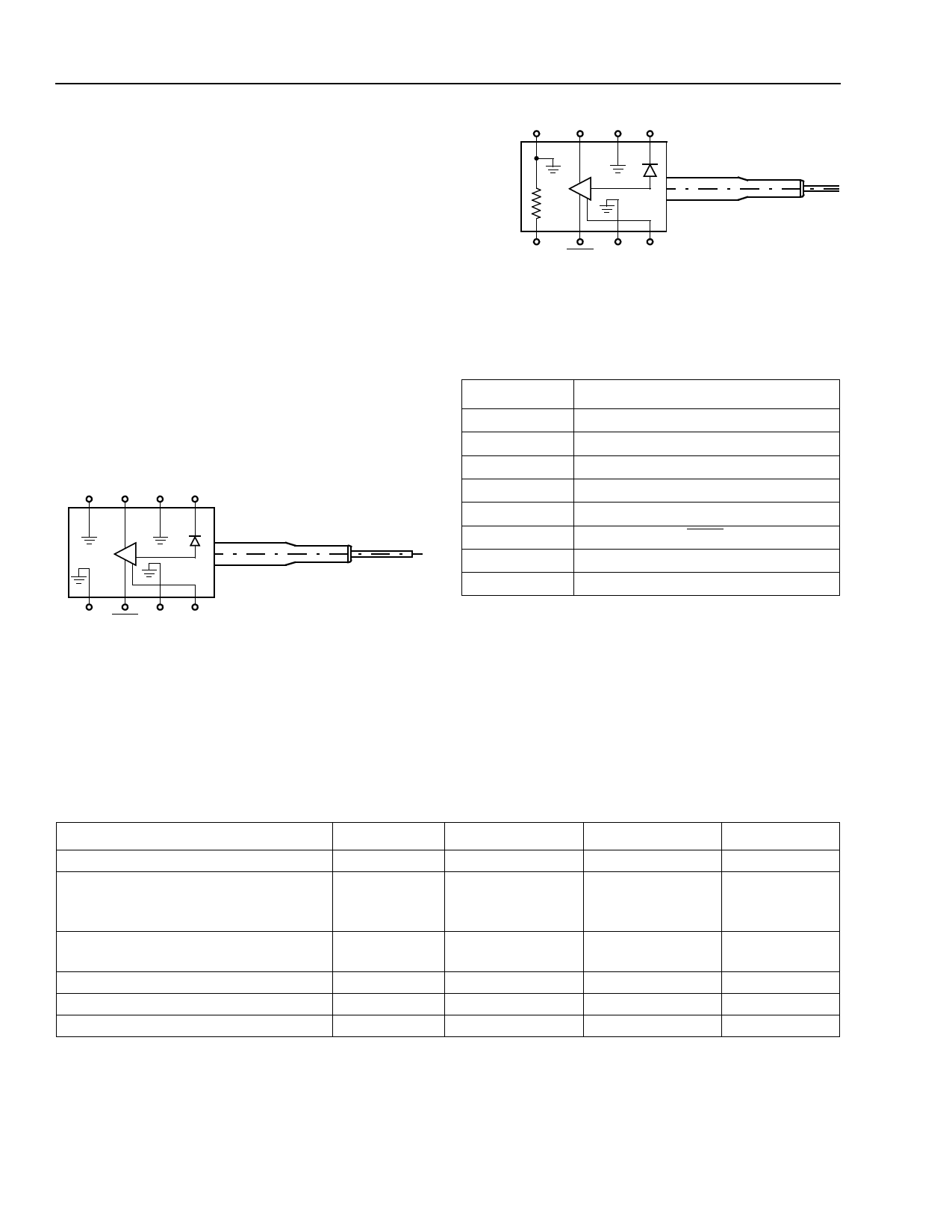
GND DATA GND VPD
4
3
2
1
5
6
7
8
GND DATA GND VCC
1-902(F).b
Figure 1. P172P PIN/Preamp Schematic (Top View)
GND DATA GND VPD
4
3
2
1
5
6
7
8
THERMISTOR DATA GND VCC
1-902(F).c
Figure 2. P172A APD/Preamp (Top View)
Table 1. P172-Type PIN/Preamp and APD/Preamp
Pin Descriptions
Pin Number
Description
1
Photodiode Bias
2
Case Ground
3
DATA*
4
Case Ground
5
Thermistor/Case Ground†
6
DATA‡
7
Case Ground
8
VCC
* Logic high when light is on.
† Thermistor in APD version; case ground in PIN version
‡ Logic low when light is on.
Absolute Maximum Ratings
Stresses in excess of the absolute maximum ratings can cause permanent damage to the device. These are abso-
lute stress ratings only. Functional operation of the device is not implied at these or any other conditions in excess
of those given in the operational sections of the data sheet. Exposure to absolute maximum ratings for extended
periods can adversely affect device reliability.
Parameter
Symbol
Min
Positive Supply Voltage
VCC
–0.5
Optical Input Power:
APD
PIN
PIN
—
PIN
—
Operating Case Temperature Range:
APD/PIN
TC
–40
Storage Temperature Range
Tstg
–40
Lead Soldering Temperature
—
—
Lead Soldering Time
—
—
Max
Unit
4.0
V
0
dBm
8.0
dBm
85
°C
85
°C
250
°C
10
s
2
Agere Systems Inc.
Share Link: 