P4C148 Ver la hoja de datos (PDF) - Semiconductor Corporation
Número de pieza
componentes Descripción
Lista de partido
P4C148 Datasheet PDF : 10 Pages
| |||
P4C148/P4C149
AC CHARACTERISTICS—READ CYCLE
(VCC = 5V ± 10%, All Temperature Ranges)(2)
-10
-12
-15
-20
-25
-35
-45
-55
Sym
Pa ra m e te r
Min Max Min Max Min Max Min Max Min Max Min Max Min Max Min Max
tRC Read Cycle Time
10
12
15
20
25
35
45
55
tAA Address Access Time
10
12
15
20
25
35
45
55
tAC Chip Enable Access Time (P4C148)
10
12
15
20
25
35
45
55
tAC Chip Enable Access Time (P4C149)
8
10
12
14
15
20
20
25
tOH Output Hold from Address Change
3
3
3
3
3
3
3
3
tLZ Chip Enable to Output in Low Z (P4C149) 2
2
2
2
2
2
2
2
tHZ Chip Disable to Output in High Z (P4C149)
4
5
6
8
10
14
18
20
tRCS Read Command Setup Time
0
0
0
0
0
0
0
0
tRCH Read Command Hold Time
0
0
0
0
0
0
0
0
tPU Chip Enable to Power Up Time (P4C148)
0
0
0
0
0
0
0
0
tPD Chip Disable to Power Down Time (P4C148)
10
12
15
20
25
35
45
55
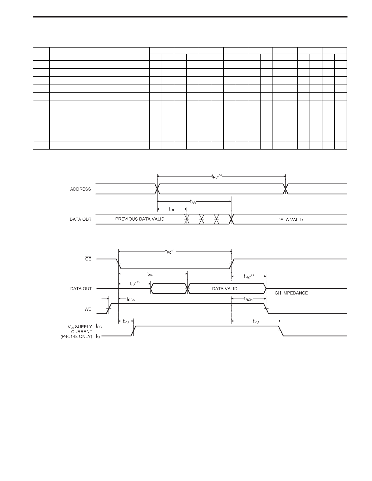
TIMING WAVEFORM OF READ CYCLE
TIMING WAVEFORM OF READ CYCLE NO. 2(6)
Notes:
1. Stresses greater than those listed under MAXIMUM RATINGS may
cause permanent damage to the device. This is a stress rating only
and functional operation of the device at these or any other
conditions above those indicated in the operational sections of this
specification is not implied. Exposure to MAXIMUM rating condi-
tions for extended periods may affect reliability.
2. Extended temperature operation guaranteed with 400 linear feet
per minute of air flow.
3. Transient inputs with VIL and IIL not more negative than –3.0V and
–100mA, respectively, are permissible for pulse widths up to 20ns.
4. This parameter is sampled and not 100% tested.
5. CE is LOW and WE is HIGH for READ cycle.
6. WE is HIGH, and address must be valid prior to or coincident with
CE transition LOW.
7. Transition is measured ±200mV from steady state voltage prior to
change with specified loading in Figure 1. This parameter is
sampled and not 100% tested.
8. Read Cycle Time is measured from the last valid address to the first
transitioning address.
Document # SRAM104 REV B
Page 3 of 10
Share Link: 