P4C188 Ver la hoja de datos (PDF) - Semiconductor Corporation
Número de pieza
componentes Descripción
Lista de partido
P4C188 Datasheet PDF : 12 Pages
| |||
P4C188/188L
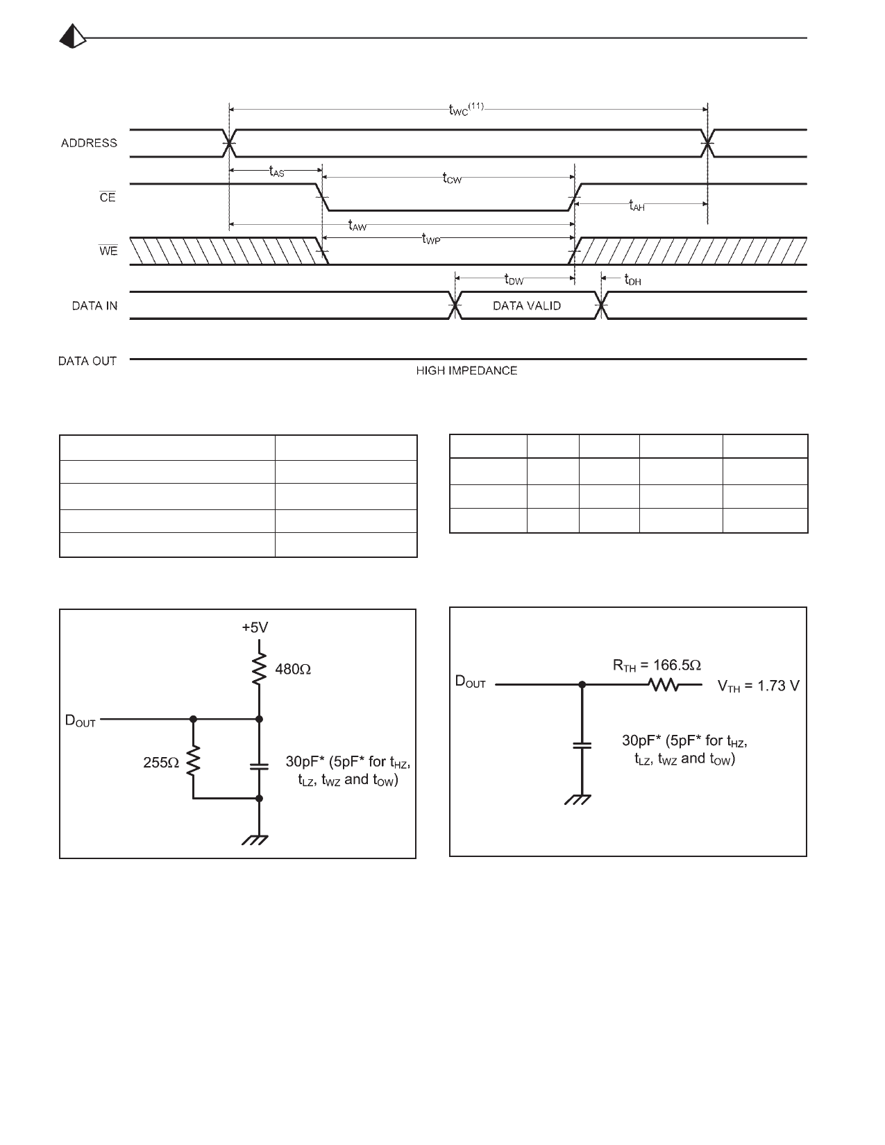
TIMING WAVEFORM OF WRITE CYCLE NO. 2 (CE CONTROLLED)(9)
AC TEST CONDITIONS
Input Pulse Levels
Input Rise and Fall Times
Input Timing Reference Level
Output Timing Reference Level
Output Load
GND to 3.0V
3ns
1.5V
1.5V
See Figures 1 and 2
TRUTH TABLE
Mode
CE
WE
Standby
H
X
Read
L
H
Write
L
L
Output
High Z
DOUT
DIN
Power
Standby
Active
Active
Figure 1. Output Load
* including scope and test fixture.
Note:
Because of the ultra-high speed of the P4C188/L, care must be taken
when testing this device; an inadequate setup can cause a normal
functioning part to be rejected as faulty. Long high-inductance leads that
cause supply bounce must be avoided by bringing the VCC and ground
planes directly up to the contactor fingers. A 0.01 µF high frequency
Figure 2. Thevenin Equivalent
capacitor is also required between VCC and ground. To avoid signal
reflections, proper termination must be used; for example, a 50Ω test
environment should be terminated into a 50Ω load with 1.73V (Thevenin
Voltage) at the comparator input, and a 116Ω resistor must be used in
series with DOUT to match 166Ω (Thevenin Resistance).
Document # SRAM112 REV A
Page 6 of 12
Share Link: 