PCA9561D Ver la hoja de datos (PDF) - Philips Electronics
Número de pieza
componentes Descripción
Lista de partido
PCA9561D Datasheet PDF : 17 Pages
| |||
Philips Semiconductors
Quad 6-bit multiplexed I2C EEPROM DIP switch
Product data sheet
PCA9561
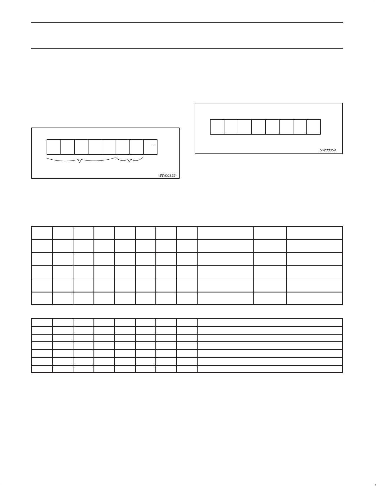
DEVICE ADDRESS
Following a START condition the bus master must output the
address of the slave it is accessing. The address of the PCA9561 is
shown in Figure 1. To conserve power, no internal pull-up resistors
are incorporated on the hardware selectable address pins and they
must be pulled HIGH or LOW.
The last bit of the slave address byte defines the operation to be
performed. When set to logic 1 a read is selected while a logic 0
selects a write operation.
MSB
LSB
CONTROL REGISTER
Following the successful acknowledgement of the slave address,
the bus master will send a byte to the PCA9561, which will be stored
in the control register. This register can be written and read via the
I2C-bus.
D7 D6 D5 D4 D3 D2 D1 D0
1
0
0
1
1 A1 A0 R/W
FIXED
PROGRAMMABLE
Figure 1. Slave address
SW00955
Figure 2. Control Register
SW00954
CONTROL REGISTER DEFINITION
Following the address and acknowledge bit with logic 0 in the read/write bit, the first byte written is the command byte. If the command byte is
reserved and therefore not valid, it will not be acknowledged. Only valid command bytes will be acknowledged.
Table 1. Register Addresses
D7
D6
D5
D4
D3
D2
D1
D0
REGISTER
NAME
0
0
0
0
0
0
0
0 EEPROM 0
0
0
0
0
0
0
0
1 EEPROM 1
0
0
0
0
0
0
1
0 EEPROM 2
0
0
0
0
0
0
1
1 EEPROM 3
1
1
1
1
1
1
1
1 MUX_IN
TYPE
Read/Write
Read/Write
Read/Write
Read/Write
Read
REGISTER
FUNCTION
EEPROM byte 0
register
EEPROM byte 1
register
EEPROM byte 2
register
EEPROM byte 3
register
MUX_IN values
register
Table 2. Commands
D7
D6
D5
D4
D3
D2
D1
D0
COMMAND
1
1
1
1
1
0
0
0 MUX_OUT from EEPROM byte 0
1
1
1
1
1
1
0
0 MUX_OUT from EEPROM byte 1
1
1
1
1
1
0
X
1 MUX_OUT from EEPROM byte 2
1
1
1
1
1
1
X
1 MUX_OUT from EEPROM byte 3
1
1
1
1
1
X
1
0 MUX_OUT from MUX_IN
1
1
1
1
1
X
X
1 MUX_OUT from MUX_SELECT2
NOTE:
1. All other combinations are reserved.
2. MUX_SELECT pins select between MUX_IN and EEPROM to MUX_OUT.
2004 May 17
4
Share Link: 