PCD5032H Ver la hoja de datos (PDF) - Philips Electronics
Número de pieza
componentes Descripción
Lista de partido
PCD5032H Datasheet PDF : 24 Pages
| |||
Philips Semiconductors
ADPCM CODEC for digital cordless
telephones
Product specification
PCD5032
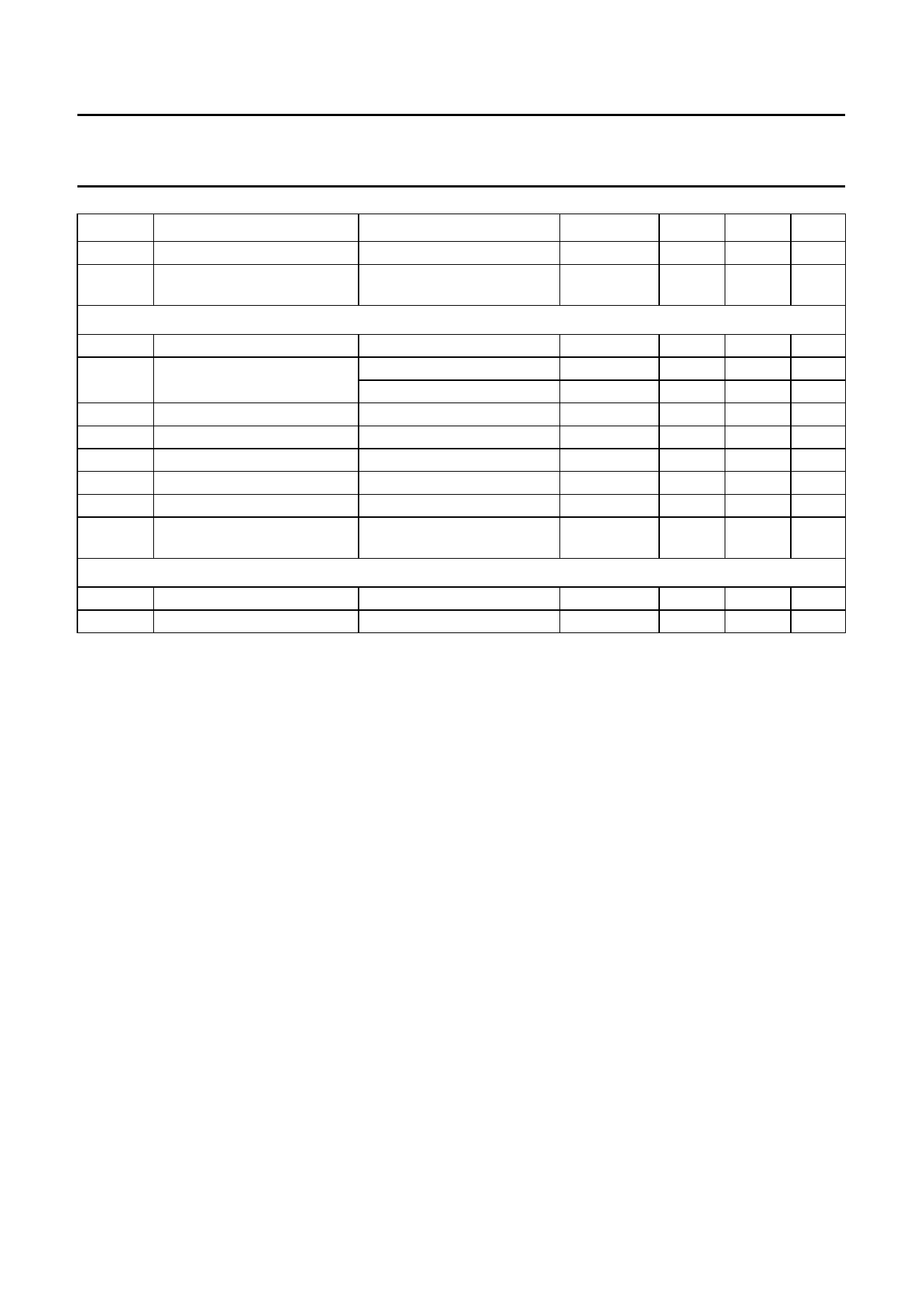
SYMBOL
PARAMETER
CONDITIONS
MIN.
TYP. MAX. UNIT
Gv(step)
THDTX
voltage gain, step size
total harmonic distortion
(transmitted)
note 9
−
1
−
dB
−
−
−40
dB
Receiver audio output
Zo
output impedance
note 6
−
10
−
Ω
Vo(rms)
output signal level (RMS
0 dBm0; note 10
−
value)
3.14 dBm0; note 11
−
550
−
mV
1250 −
mV
Gv(min) minimum voltage gain
−4
−3
−2
dB
Gv(max) maximum voltage gain
+3
+4
+5
dB
Gv(step)
voltage gain, step size
−
1
−
dB
Gvol
volume control range
−36
−
0
dB
Gvol(step) volume step size
−
6.0
−
dB
THDRX
total harmonic distortion
(received)
note 12
−
−
−40
dB
Ringer output; notes 5 and 13
Zo
output impedance
Gvol
volume control range
−
14
29
Ω
−29
−
+4
dB
Notes
1. All outputs left open. IDD measured with all inputs connected to VSS, except: CLK and DCLK connected to 3.456 MHz;
RAS and TAS connected to 8 kHz. Istb measured with all inputs connected to VSS, except: TM+, TM− left open.
2. The reference voltage is available on VREF+ and VREF− and is measured with respect to VGA. The voltage outputs
are intended for electret microphone supply and can deliver 400 µA.
3. Digital inputs and outputs are CMOS-levels compatible. The outputs and inputs can sink or source 1 mA. Pull-down
resistors are present at pins RPI, TPI, TEST, RAD.
4. Any frequency between min. and max. is allowed for DCLK. The signals CLK and RAS/TAS must be
frequency-locked and will have a ratio of fCLK/fRAS = 432
5. All analog input/output voltages are measured differentially. The circuit is designed for use with an electret
microphone.
6. Frequency band is 300 Hz to 3400 Hz. Maximum load capacitance = 100 pF differentially, or 200 pF each pin.
7. Nominal signal level gives −10 dBm0 on the PCM interface (G.711/G.712). Value given for TX gain setting 0 dB.
8. Nominal signal level gives 3.14 dBm0 on the PCM interface, with larger input signals the digital output will be
saturated. Value given for TX gain setting 0 dB.
9. Transmitter gain setting = 0 dB and input signal level = 40 mV (RMS) (will generate 0 dBm0 on PCM interface
according to G.711).
10. PCM signal level is 0 dBm0 and RX gain setting 0 dB. With a load of 300 Ω between RE+ and RE− the signal level
results in an output power of 1 mW. The maximum output current is 10 mA.
11. PCM signal level is +3.14 dBm0 and RX gain setting +4 dB. The maximum output current is 10 mA.
12. PCM signal level is 0 dBm0 (G.711).
13. For maximum output power the load resistance should equal the typical output impedance (specified at
ILOAD −20 mA). The absolute maximum value of output power given in Chapter 9 defines the minimum load
resistance.
1997 Apr 03
15
Share Link: 