PCD5043 Ver la hoja de datos (PDF) - Philips Electronics
Número de pieza
componentes Descripción
Lista de partido
PCD5043 Datasheet PDF : 24 Pages
| |||
Philips Semiconductors
DECT burst mode controller
Objective specification
PCD5043
SYMBOL
VSS3
DO
FS1
FS2
DI
DCK
CLK3
ANT_SW
T_ENABLE
T_POWER_RMP
RMT_STAT
SYNTH_LOCK
VSS4
REF_CLK
VDD2
S_ENABLE
S_CLK
S_DATA
S_POWER_DWN
VCO_BND_SW
1200 HZ
T_DATA
SET_OFF_IN
TEST1
RSSI_AN
TEST2
TEST3
R_DATA
R_ENABLE
R_POWER_DWN
SLICE_CTR
VDD3
VSS5
VREF
VDD(RAM)
SYNCPORT
1996 Oct 31
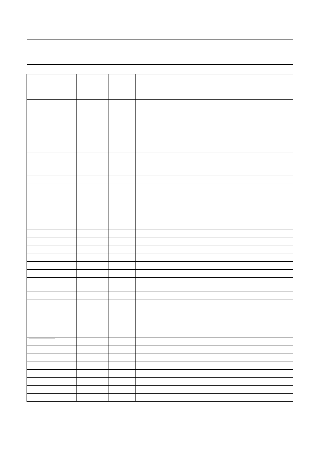
PIN
TYPE(1)
DESCRIPTION
26
P
negative supply 3
27
O
3-state data output on the speech interface
28
I/O 8 kHz framing signal to ADPCM CODEC 1 output, for simple base +
handset, otherwise 8 kHz framing input
29
O
8 kHz framing signal to ADPCM CODEC 2 in the base station mode
30
I
data input on the speech interface
31
O
simple base + handset; 1152 kHz data clock (output), otherwise
2048 kHz data clock (input) signal
32
O
3.456 MHz clock (nominal value, used to adjust system timing)
33
O
selects one of two antennas
34
O
Transmitter Enable (active LOW)
35
O
Transmitter Power Ramp control
36
I
serial 8-bit data can be read in for each slot; REMote radio
37
I
lock indication from synthesizer
38
P
negative supply 4
39
O
reference frequency for the synthesizer, i.e. the crystal oscillator
clock fCLK
40
P
positive supply 2
41
O
synthesizer enable
42
O
clock signal, to be used with S_DATA
43
O
serial data to the synthesizer
44
O
synthesizer power-down control
45
O
VCO bandswitch control signal
46
O
control signal for dual synthesizer schemes
47
O
serial output data to transmitter
48
I
switches off the crystal oscillator, and prevents all RF signals from
becoming active
49
I
selects various test modes.; normal operation set to 0
50
I
analog signal (for basic DECT systems), peak signal strength
measured after a lowpass filter
51
I
selects various test modes; normal operation set to 0
52
I
selects various test modes; normal operation set to 0
53
I
receive data
54
O
receiver enable (active LOW)
55
O
receiver power-down
56
O
slice time constant control
57
P
positive supply 3
58
P
negative supply 5
59
I
reference input for the A/D converter
60
P
power supply for data RAM
61
I/O in the base station the signal is the SYNCPORT
5
Share Link: 