PCF8573 Ver la hoja de datos (PDF) - Philips Electronics
Número de pieza
componentes Descripción
Lista de partido
PCF8573 Datasheet PDF : 28 Pages
| |||
Philips Semiconductors
Clock/calendar with serial I/O
Product specification
PCF8573
9 I2C-BUS PROTOCOL
9.1 Addressing
Before any data is transmitted on the I2C-bus, the device which should respond is addressed first. The addressing is
always done with the first byte transmitted after the start procedure.
The clock/calendar acts as a slave receiver or slave transmitter. Therefore the clock signal SCL is only an input signal,
but the data signal SDA is a bidirectional line.
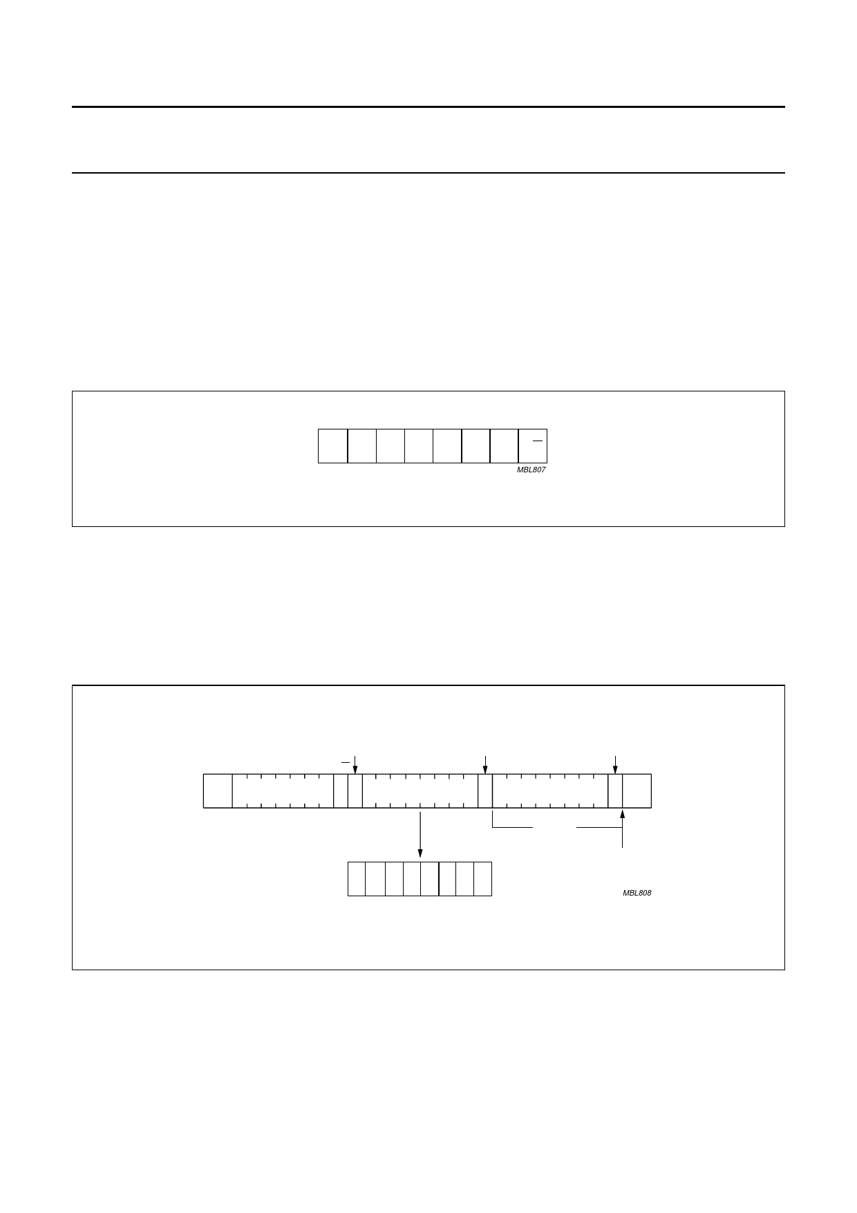
The clock/calendar slave address is shown in Fig.8. Bits A0 and A1 correspond to the two hardware address pins A0 and
A1. Connecting these to VDD or VSS allows the device to have 1 of 4 different addresses.
handbook, halfpamgesb
lsb
1 1 0 1 0 A1 A0 R/W
MBL807
Fig.8 Slave address.
9.2 Clock/calendar READ/WRITE cycles
The I2C-bus configuration for different clock/calendar READ and WRITE cycles is shown in Figs 9, 10 and 11.
The write cycle is used to set the time counter, the alarm register and the flags. The transmission of the clock/calendar
address is followed by the MODE-POINTER-word which contains a CONTROL-nibble (Table 3) and an
ADDRESS-nibble (Table 4). The ADDRESS-nibble is valid only if the preceding CONTROL-nibble is set to EXECUTE
ADDRESS. The third transmitted word contains the data to be written into the time counter or alarm register.
handbook, full pagewidth
acknowledge
from slave
acknowledge
from slave
R/W
S
CLOCK/CALENDAR
ADDRESS
0
A
MODE POINTER
msb
A
DATA
acknowledge
from slave
lsb
AP
0 C2 C1 C0 0 B2 B1 B0
n bytes
(n = 0, 1, 2, ...)
auto increment
of B1, B0
MBL808
Fig.9 Master transmitter transmits to clock/calendar slave receiver.
2003 Jan 27
9
Share Link: 