PCK2022RADGG Ver la hoja de datos (PDF) - Philips Electronics
Número de pieza
componentes Descripción
Lista de partido
PCK2022RADGG
Philips Electronics

PCK2022RADGG Datasheet PDF : 14 Pages
| |||
Philips Semiconductors
CK00 (100/133 MHz) spread spectrum differential
system clock generator
Product data
PCK2022RA
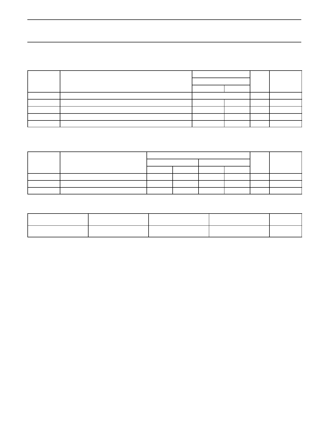
REF clock output
Tamb = 0 to +70 °C; lump capacitance test load = 20 pF
SYMBOL
PARAMETER
f
Frequency, actual
tHKL
tHKH
tJITTER
DUTY CYCLE
REFCLK LOW time
REFCLK HIGH time
Cycle-to-cycle jitter
Output duty cycle
REFER TO NOTES ON PAGE 9.
All outputs
Tamb = 0 to +70 °C
SYMBOL
PARAMETER
tPZL, tPZH
Output enable delay (all outputs)
tPZL, tPZH
Output disable delay (all outputs)
tSTABLE
All clock stabilization from power-up
REFER TO NOTES ON PAGE 9.
Group offset limits
GROUP
Host to IOCLK
OFFSET
1.5 - 3.5 ns
Host leads
LIMITS
48 MHz MODE
MIN
MAX
14.318
30
37
30
37
—
300
45
55
UNITS
MHz
ns
ns
ps
%
NOTES
17, 20
20
20
18, 20
18, 20
LIMITS
133 MHz MODE
100 MHz MODE
MIN
MAX
MIN
MAX
1.0
10.0
1.0
10.0
1.0
10.0
1.0
10.0
—
3
—
3
UNITS
ns
ns
ms
NOTES
20
20
7, 20
MEASUREMENT LOADS
(LUMPED)
IOCLK @ 30 pF
MEASUREMENT POINTS
Host @ Cross point
IOCLK @ 1.5 V
NOTES
19, 20
NOTES TO THE AC TABLES:
1. Output drivers must have monotonic rise/fall times through the specified VOL/VOH levels.
2. Period, jitter, offset, and skew measured on rising edge at 1.5 V for 3.3 V clocks.
3. The IOCLK clock is the Host clock divided by 4 in 33 MHz mode and divided by 2 in 66 MHz mode at Host = 133 MHz.
IOCLK clock is the Host clock divided by 3 in 33 MHz and divided by 2/3 in 66 MHz mode at Host = 100 MHz.
4. Frequency accuracy of 48 MHz must be +167 ppm to match USB default.
5. tHKH is measured at 2.4 V for 3.3 V outputs, as shown in Figure 7.
6. tHKL is measured at 0.4 V for all outputs as shown in Figure 7.
7. the time is specified from when VDDQ achieves its normal operating level (typical condition VDDQ = 3.3 V) until the frequency output is stable
and operating within specification.
8. tRISE and tFALL are measured as a transition through the threshold region VOL = 0.4 V and VOH = 2.4 V (1 mA) JEDEC specification.
9. The average period over any 1 µs period of time must be greater than the minimum specified period.
10. Calculated at minimum edge rate (1 V/ns) to guarantee 45-55% duty cycle. Pulse width is required to be wider at faster edge rate to ensure
duty specification is met.
11. Test load is RS = 33.2 Ω, RP = 49.9 Ω.
12. Must be guaranteed in a realistic system environment.
13. Configured for VOH = 0.71 V in a 50 Ω environment.
14. Measured at crossing points.
15. Measured at 20% to 80%.
16. Determined as a fraction of 2*(tRP - tRN) / (tRP + tRN), where tRP is a rising edge, and tRN is an intersecting falling edge.
17. Frequency generated by crystal oscillator
18. Voltage measure point (VM = 1.5 V). VDD = 3.3 V.
19. All offsets are to be measured at rising edges.
20. Parameters are guaranteed by design.
2003 Jul 31
9
Share Link: