4241 Ver la hoja de datos (PDF) - Peregrine Semiconductor Corp.
Número de pieza
componentes Descripción
Lista de partido
4241 Datasheet PDF : 8 Pages
| |||
Evaluation Kit
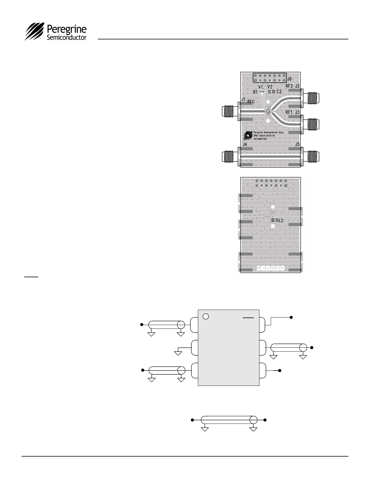
The SPDT Switch Evaluation Kit board was
designed to ease customer evaluation of the
PE4241 SPDT switch. The RF common port is
connected through a 50Ω transmission line to the
top left SMA connector, J1. Port 1 and Port 2 are
connected through 50Ω transmission lines to the
top two SMA connectors on the right side of the
board, J3 and J2, respectively. A through
transmission line connects SMA connectors J4
and J5. This transmission line can be used to
estimate the loss of the PCB over the
environmental conditions being evaluated.
The board is constructed of a two metal layer FR4
material with a total thickness of 0.031”. The
bottom layer provides ground for the RF
transmission lines. The transmission lines were
designed using a coplanar waveguide with ground
plane model using a trace width of 0.0476”, trace
gaps of 0.030”, dielectric thickness of 0.028”,
metal thickness of 0.0021” and εr of 4.4.
J6 provides a means for controlling DC and digital
inputs to the device. Starting from the lower left
pin, the second pin to the right (J6-3) is connected
to the device V1 or CTRL input. The fourth pin to
the right (J6-7) is connected to the device V2 or
CTRL/VDD input.
J3
J2
PE4241
Product Specification
Figure 4. Evaluation Board Layout
Figure 5. Evaluation Board Schematic
RF1
GND
CTRL
or VDD
RFC
J6-7
J1
RF2
CTRL
J6-3
©2005 Peregrine Semiconductor Corp. All rights reserved.
Page 4 of 8
J4
J5
Document No. 70-0094-01 │ UltraCMOS™ RFIC Solutions
Share Link: 