PE42693 Ver la hoja de datos (PDF) - Peregrine Semiconductor Corp.
Número de pieza
componentes Descripción
Lista de partido
PE42693 Datasheet PDF : 4 Pages
| |||
PE42693
Product Brief
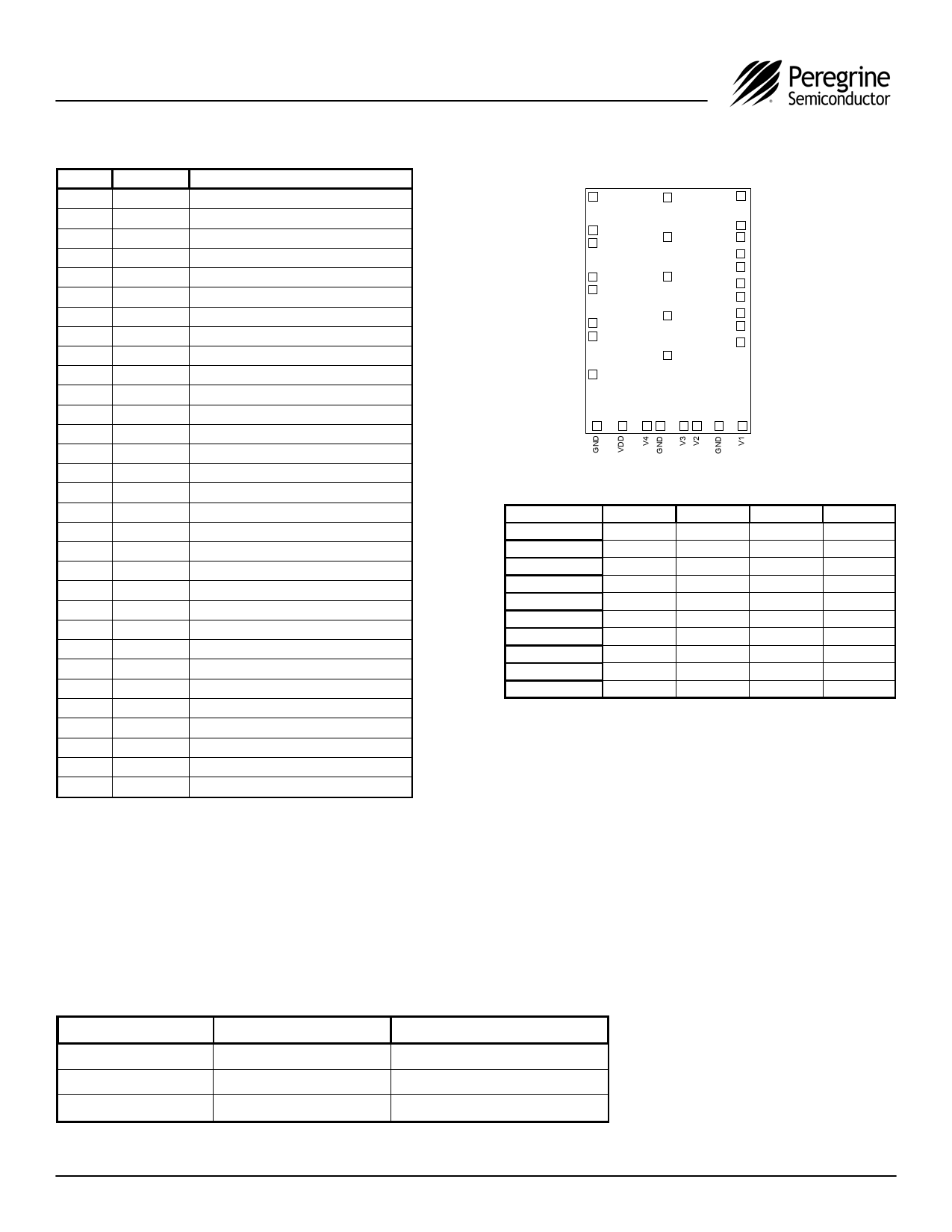
Table 4. Pin Descriptions
Pad #
1
2
3
4
5
6
7
8
9
10
11
12
13
14
15
16
17
18
19
20
21
22
23
24
25
26
27
28
29
30
31
Pad Name
TRX37
GND6
RX17
GND6
RX27
GND6
RX37
GND6
RX47
GND6
V18
GND6
V28
V38
GND6
V48
VDD8
GND6
GND6
TX27
GND6
TX17
GND6
TRX27
GND6
TRX17
ANT9
ANT9
ANT9
ANT9
ANT9
Description
RF I/O – TRX3
Ground
RF I/O – RX1
Ground
RF I/O – RX2
Ground
RF I/O – RX3
Ground
RF I/O – RX4
Ground
Switch control input, CMOS logic level
Ground
Switch control input, CMOS logic level
Switch control input, CMOS logic level
Ground
Switch control input, CMOS logic level
Supply
Ground
Ground
RF I/O – TX2
Ground
RF I/O – TX1
Ground
RF I/O – TRX2
Ground
RF I/O – TRX1
RF Common – Antenna
RF Common – Antenna
RF Common – Antenna
RF Common – Antenna
RF Common – Antenna
Notes: 6. GND traces should be physically short and connected to
ground plane for best performance.
7. Blocking capacitors needed only when non-zero DC
voltage present.
8. Application must ensure at least 40 dB of voltage isolation
from the RF signal.
9. Redundant antenna pads for flexible impedance matching.
Figure 4. Pad Configuration (Top View)
TRX1 26
GND 25
TRX2 24
GND 23
TX1 22
GND 21
TX2 20
GND 19
27 ANT
28
ANT
29 ANT
30 ANT
31 ANT
1 TRX3
2 GND
3 RX1
4 GND
5 RX2
6 GND
7 RX3
8 GND
9 RX4
10 GND
18
17
16 15
14 13
12
11
Table 5. Truth Table
Path
RX1-ANT
RX2-ANT
RX3-ANT
RX4-ANT
TX1-ANT
TX2-ANT
TRX1-ANT
TRX2-ANT
TRX3-ANT
ALL Off
V4
0
0
0
0
0
0
1
0
1
Note
V3
0
0
0
0
1
1
1
1
0
Note
V2
0
0
1
1
0
1
0
0
0
Note
Note: All unused logic states will turn all RF ports off.
V1
0
1
0
1
1
0
0
0
1
Note
Electrostatic Discharge (ESD) Precautions
When handling this UltraCMOS™ device, observe
the same precautions that you would use with other
ESD-sensitive devices. Although this device
contains circuitry to protect it from damage due to
ESD, precautions should be taken to avoid
exceeding the specified rating.
Latch-Up Avoidance
Unlike conventional CMOS devices, UltraCMOS™
devices are immune to latch-up.
Table 6. Ordering Information
Order Code
PE42693DTI
PE42693DBI
EK-42693-01
Package
Wafer on Film Frame
Die in Waffle Pack
Evaluation Kit
Shipping Method
Wafer (Gross Die / Wafer Quantity)
238 Dice / Waffle Pack
1/ box
Document No. 70-0231-01 │ www.psemi.com
Contact sales@psemi.com for full version of datasheet
©2007 Peregrine Semiconductor Corp. All rights reserved.
Page 3 of 4
Share Link: 