RT8101 Ver la hoja de datos (PDF) - Richtek Technology
Número de pieza
componentes Descripción
Lista de partido
RT8101 Datasheet PDF : 15 Pages
| |||
RT8101/A
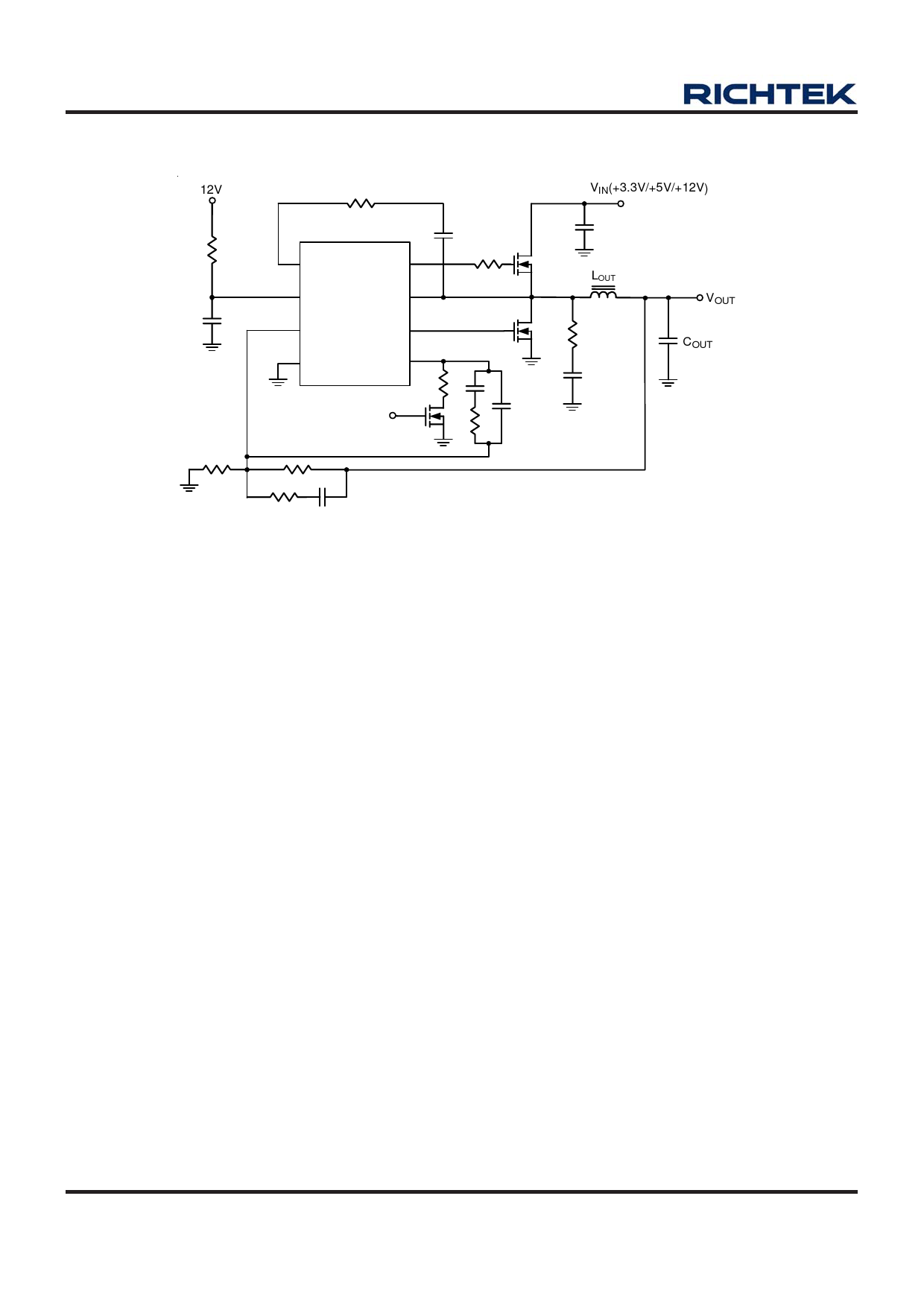
Typical Application Circuit
Preliminary
12V
RBOOT
VIN(+3.3V/+5V/+12V)
RT8101/A
1 BOOT UGATE 2
5 VCC
8
PHASE
6 FB
LGATE 4
3 GND
COMP 7
RUGATE
Q1
CIN
LOUT
Q2 R
C
VOUT
COUT
PSC
Functional Pin Description
BOOT (Pin 1)
Bootstrap supply for the upper gate driver. Connect the
bootstrap capacitor between BOOT pin and the PHASE
pin. The bootstrap capacitor provides the charge to turn
on the upper MOSFET.
UGATE (Pin 2)
Upper gate driver output. Connect to gate of the high-
side power N-Channel MOSFET. This pin is monitored by
the adaptive shoot-through protection circuitry to
determine when the upper MOSFET is turned off.
GND (Pin 3)
Signal ground for the IC.
LGATE (Pin 4)
Lower gate driver output. Connect to the gate of the low-
side power N-Channel MOSFET. This pin is monitored by
the adaptive shoot-through protection circuitry to determine
when the lower MOSFET is turned off.
VCC (Pin 5)
Connect this pin to a well-decoupled 12V bias supply. It
is also the positive supply for the lower gate driver, LGATE.
FB (Pin 6)
Buck converter feedback voltage. This pin is the inverting
input of the error amplifier. FB senses the switcher output
through an external resistor divider network.
COMP (Pin 7)
Buck converter external compensation. This pin is used
to compensate the control loop of the buck converter.
PHASE (Pin 8)
Connect this pin to the source of the upper MOSFET and
the drain of the lower MOSFET. This pin is monitored by
the adaptive shoot-through protection circuitry to
determine when the upper MOSFET is turned off.
Exposed Pad
Exposed pad should be soldered to PCB board and
connected to GND.
www.richtek.com
2
DS8101/A-01 March 2007
Share Link: 