CS8413 Ver la hoja de datos (PDF) - Cirrus Logic
Número de pieza
componentes Descripción
Lista de partido
CS8413 Datasheet PDF : 38 Pages
| |||
CS8413 CS8414
status register 1 to generate an interrupt pulse. A
“0” masks that particular status bit from causing an
interrupt.
Status register 2 (SR2) reports all the conditions
that can affect the error flag bit in SR1 and the error
pin (ERF), and can specify the received clock fre-
quency. As previously mentioned, the first five bits
of SR2 are AND’ed with their interrupt enable bits
(in IER2) and then OR’ed to create ERF. The V,
PARITY, CODE and LOCK bits are latches which
are set when their corresponding conditions occur,
and are reset when SR2 is read. The ERF pin is as-
serted each time the error occurs assuming the in-
terrupt enable bit in IER2 is set for that particular
error. When the ERF pin is asserted, the ERF bit in
SR1 is set. If the ERF bit was not set prior to the
ERF pin assertion, an interrupt will be generated
(assuming bit 3 in IER1 is set). Although the ERF
pin is asserted for each occurrence of an enabled er-
ror condition, the ERF bit will only cause an inter-
rupt once if SR1 is not read.
X:01 7
6
5
4
3
2
1
0
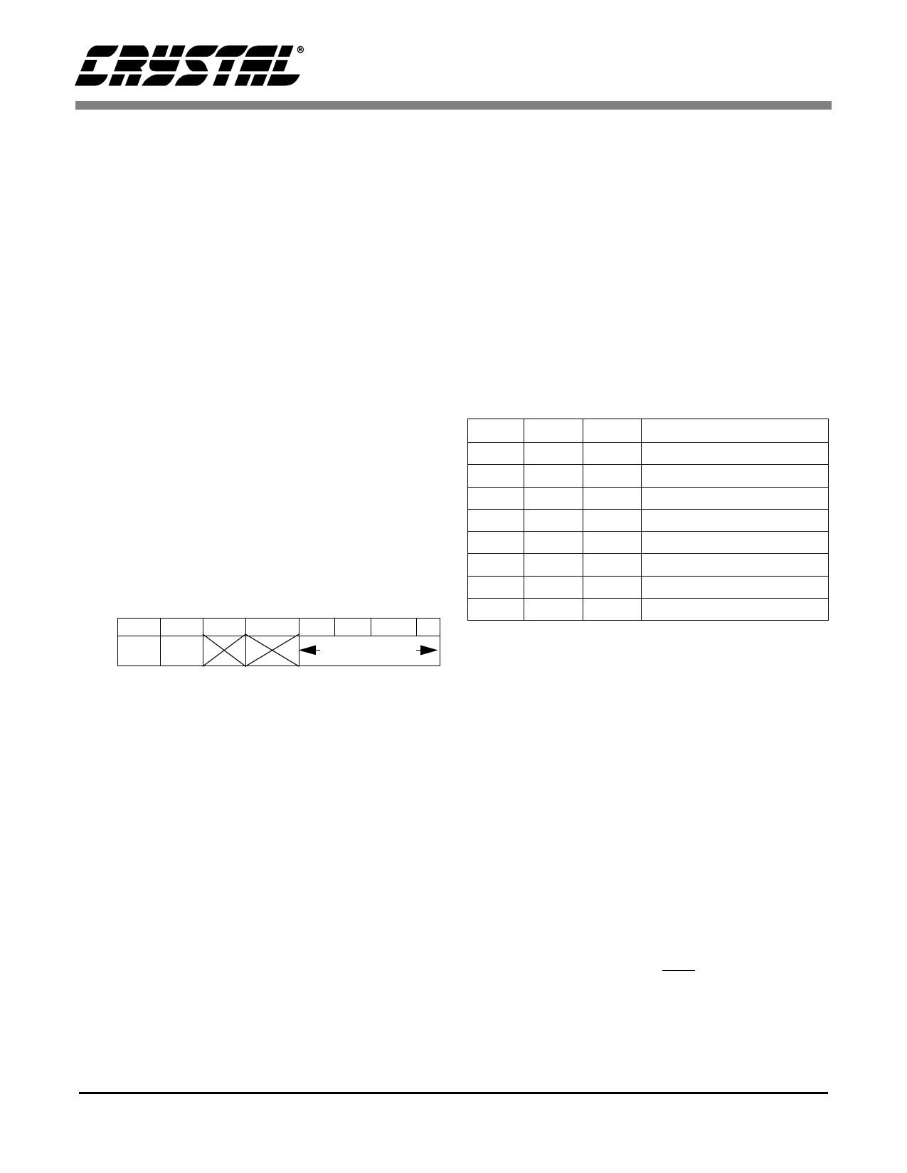
SR2. FREQ2 FREQ1 FREQ0 Reserved LOCK CODE PARITY V
IER2. TEST1 TEST0
INT. ENABLE BITS
FOR ABOVE
SR2:
FREQ2:
FREQ1:
FREQ0:
LOCK:
CODE:
PARITY:
V:
The 3 FREQ bits indicate incoming sample frequency.
(must have 6.144 MHz clock on FCK pin and FCEN
must be “1”)
Out-of-Lock error
Coding violation
Parity error
Validity bit high
IER2: TEST1,0: (0 on power-up) Must stay at “0”.
INT. ENABLES: Enables the corresponding bit in SR2.
A “1” enables the interrupt. A “0” masks the interrupt.
Figure 7. Status/IEnable Register 2
V is the validity status bit which is set any time the
received validity bit is high. PARITY is set when a
parity error is detected. CODE is set when a bi-
phase coding error is detected. LOCK is asserted
when the receiver PLL is not locked and occurs
when there is no input on RXP/RXN, or if the re-
ceived frequency is out of the receiver lock range
(28.4 kHz to 100 kHz).
The upper three bits in SR2, FREQ2-FREQ0, can
report the receiver frequency when the receiver is
locked. These bits are only valid when FCEN in
control register 1 is set, and a 6.144 MHz clock is
applied to the FCK pin. When FCEN is set, the
A4/FCK pin is used as FCK and A4 is internally set
to zero; therefore, only the lower half of the buffer
can be accessed. Table 1 lists the frequency ranges
reported. The FREQ bits are updated three times
per block and the clock on the FCK pin must be val-
id for two thirds of a block for the FREQ bits to be
accurate. The FREQ bits are invalid when the PLL
is out of lock.
FREQ2 FREQ1 FREQ0
0
0
0
0
0
1
0
1
0
0
1
1
1
0
0
1
0
1
1
1
0
1
1
1
Sample Frequency
Out of Range
reserved
reserved
96 kHz ± 4%
88.2 kHz ± 4%
48 kHz ± 4%
44.1 kHz ± 4%
32 kHz ± 4%
Table 1. Incoming Sample Frequency Bits
IEnable register 2 has corresponding interrupt en-
able bits for the first five bits in SR2. A “1” enables
the condition in SR2 to cause ERF to go high, while
a “0” masks that condition. Bit 5 is unused and bits
6 and 7, the two most significant bits, are factory
test bits and must be set to zero when writing to this
register. The CS8413 sets these bits to zero on pow-
er-up.
Control Registers
The CS8413 contains two control registers. Control
register 1 (CR1), at address 2, selects system level
features, while control register 2 (CR2), at address
3, configures the audio serial port.
In control register 1, when RST is low, all outputs
are reset except MCK (FSYNC and SCLK are high
impedance). The CS8413 should be reset imediate-
ly after power-up and any time the user performs a
DS240F1
11
Share Link: 