CS8413 Ver la hoja de datos (PDF) - Cirrus Logic
Número de pieza
componentes Descripción
Lista de partido
CS8413 Datasheet PDF : 38 Pages
| |||
CS8413 CS8414
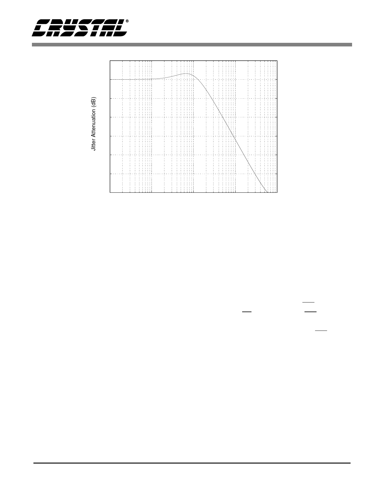
5
0
-5
-10
-15
-20
-25
-30102
103
104
105
106
Jitter Frequency (Hz)
Figure 3. Typical Jitter Attenuation Characteristics
are extracted at times when intersymbol interfer-
ence is at a minimum. This provides a sample fre-
quency clock that is as spectrally pure as the digital
audio source clock for moderate length transmis-
sion lines. For long transmission lines, the CS8413
can be programmed to generate FSYNC from
MCK instead of from the incoming data.
CS8413 DESCRIPTION
The CS8413 is more flexible than the CS8414 but
requires a microcontroller or DSP to load internal
registers. The CS8414 does not have internal regis-
ters so it may be used in a stand-alone mode where
a microprocessor or DSP is not available.
The CS8413 accepts data from a transmission line
coded according to the digital audio interface stan-
dards. The I.C. recovers clocks and data, and sepa-
rates the audio data from control information. The
audio data is output through a configurable serial
port and the control information is stored in internal
dual-port RAM. Extensive error reporting is avail-
able via internal registers with the option of repeat-
ing the last sample when an error occurs. A block
diagram of the CS8413 is shown in Figure 4
Parallel Port
The parallel port accesses two status registers, two
interrupt enable registers, two control registers, and
28 bytes of dual-port buffer memory. The status
registers and interrupt enable registers occupy the
same address space. A bit in control register 1 se-
lects the two registers, either status or interrupt en-
able, that occupy addresses 0 and 1 in the memory
map. The address bus and the RD/WR line should
be valid when CS goes low. If RD/WR is low, the
value on the data bus will be written into the buffer
memory at the specified address. If RD/WR is high,
the value in the buffer memory, at the specified ad-
dress, is placed on the data bus. Detailed timing for
the parallel port can be found in the Switching
Characteristics - Parallel Port table.
The memory space on the CS8413 is allocated as
shown in Figure 5. There are three defined buffer
modes selectable by two bits in control register 1.
Further information on the buffer modes can be
found in the Control Registers section.
8
DS240F1
Share Link: 