HIP6020 Ver la hoja de datos (PDF) - Intersil
Número de pieza
componentes Descripción
Lista de partido
HIP6020 Datasheet PDF : 15 Pages
| |||
HIP6020
∆VOSC
OSC
PWM
COMP
-
+
VIN
DRIVER
LO
VOUT
DRIVER
PHASE
CO
VE/A
ZFB
-
+
ERROR
AMP
ZIN
REFERENCE
ESR
(PARASITIC)
DETAILED COMPENSATION COMPONENTS
C2
C1 R2
ZFB
VOUT
ZIN
C3 R3
R1
COMP
FB
-
+
HIP6020
DACOUT
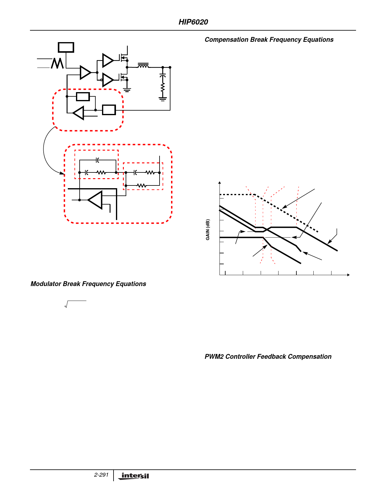
FIGURE 8. VOLTAGE-MODE BUCK CONVERTER
COMPENSATION DESIGN
The modulator transfer function is the small-signal transfer
function of VOUT/VE/A. This function is dominated by a DC
Gain, given by VIN/VOSC, and shaped by the output filter, with
a double pole break frequency at FLC and a zero at FESR.
Modulator Break Frequency Equations
FLC=
-------------------1--------------------
2π × LO × CO
FESR= 2----π-----×-----E----S--1---R------×-----C----O---
The compensation network consists of the error amplifier
(internal to the HIP6020) and the impedance networks ZIN and
ZFB. The goal of the compensation network is to provide a
closed loop transfer function with high 0dB crossing frequency
(f0dB) and adequate phase margin. Phase margin is the
difference between the closed loop phase at f0dB and 180
degrees. The equations below relate the compensation
network’s poles, zeros and gain to the components (R1, R2,
R3, C1, C2, and C3) in Figure 11. Use these guidelines for
locating the poles and zeros of the compensation network:
1. Pick Gain (R2/R1) for desired converter bandwidth
2. Place 1ST Zero Below Filter’s Double Pole (~75% FLC)
3. Place 2ND Zero at Filter’s Double Pole
4. Place 1ST Pole at the ESR Zero
5. Place 2ND Pole at Half the Switching Frequency
6. Check Gain against Error Amplifier’s Open-Loop Gain
7. Estimate Phase Margin - Repeat if Necessary
Compensation Break Frequency Equations
FZ1 = -2---π-----×-----R---1--2-----×----C-----1--
FP1
=
---------------------------1---------------------------
2π
×
R2
×
C-C----11-----+×-----CC-----22--
FZ2 = -2---π-----×-----(--R-----1-----+-1----R-----3----)---×-----C-----3-
FP2 = -2---π-----×-----R---1--3-----×----C-----3--
Figure 12 shows an asymptotic plot of the DC-DC converter’s
gain vs. frequency. The actual Modulator Gain has a high gain
peak dependent on the quality factor (Q) of the output filter,
which is not shown in Figure 12. Using the above guidelines
should yield a Compensation Gain similar to the curve plotted.
The open loop error amplifier gain bounds the compensation
gain. Check the compensation gain at FP2 with the capabilities
of the error amplifier. The Closed Loop Gain is constructed on
the log-log graph of Figure 12 by adding the Modulator Gain (in
dB) to the Compensation Gain (in dB). This is equivalent to
multiplying the modulator transfer function to the compensation
transfer function and plotting the gain.
100
FZ1
FZ2 FP1 FP2
OPEN LOOP
ERROR AMP GAIN
80
20
log
V----V-P---I--–-N----P--
60
40
COMPENSATION
GAIN
20
0
-20
20
log
RR-----21--
MODULATOR
-40
GAIN
FLC FESR
CLOSED LOOP
GAIN
-60
10
100
1K
10K 100K 1M 10M
FREQUENCY (Hz)
FIGURE 9. ASYMPTOTIC BODE PLOT OF CONVERTER GAIN
The compensation gain uses external impedance networks
ZFB and ZIN to provide a stable, high bandwidth (BW) overall
loop. A stable control loop has a gain crossing with
-20dB/decade slope and a phase margin greater than
45 degrees. Include worst case component variations when
determining phase margin.
PWM2 Controller Feedback Compensation
To reduce the number of external small-signal components
required by a typical application, the standard PWM
controller is internally stabilized. The only stability criteria
that needs to be met relates the minimum value of the output
inductor to the equivalent ESR of the output capacitor bank,
as shown in the following equation:
LOUT(MIN) = -E----S----R-2----O-×----U-π---T--×--×---B--1--W--0---1---.--7---5-
2-291
Share Link: 