ST755 Ver la hoja de datos (PDF) - STMicroelectronics
Número de pieza
componentes Descripción
Lista de partido
ST755 Datasheet PDF : 9 Pages
| |||
ST755
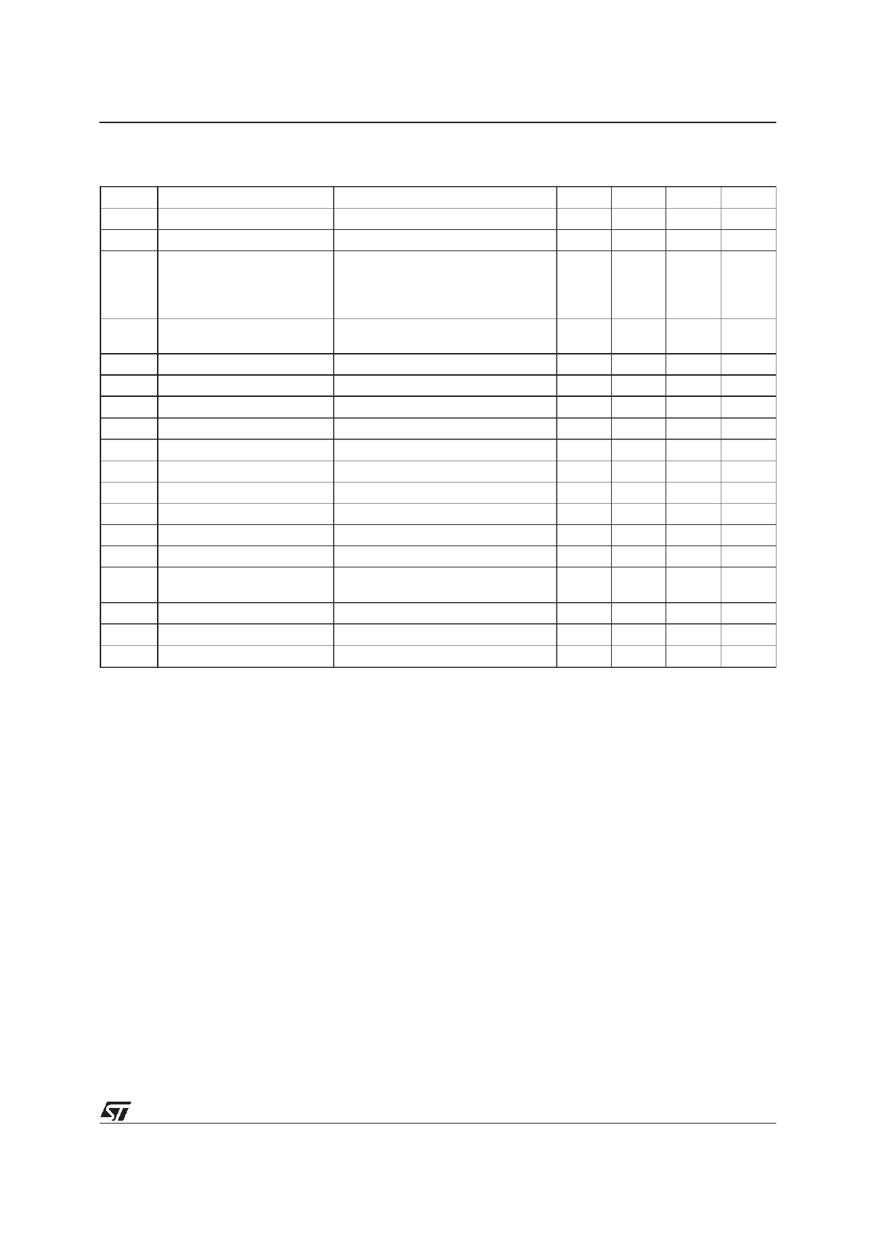
ELECTRICAL CHARACTERISTICS (Refer to the test circuits, VCC = 5V, Vout = -5.25 to -4.75V,
Iload = 0mA, Ta = Tmin to Tmax unless otherwise specified. Typical Value are referred at Ta = 25 oC)
Symbol
Parameter
Test Conditions
Min. Typ. Max. Unit
VIN Input Voltage
2.7
11
V
Vo Output Voltage
Io Output Current
Io = 0 mA to 200 mA VCC = 4.5 to 6.2 V -5.25
-5
-4.75
V
VCC = 4.5 to 6.2 V Ta = 0 oC to 70 oC
200
275
mA
VCC = 4.5 to 6.2 V Ta = -40 oC to 85 oC 175
mA
VCC = 4 V Vout = -5 V
175
mA
VCC = 2.7 V Vout = -5 V
125
mA
ISUPPLY Supply Current (Including
Switching Current)
No Load, VSHDN = VCC
1.2
3.5
mA
IOFF Standby Current
No Load, VSHDN = 0V
10
100
µA
ISC Short Circuit Current
1.2
A
∆Vo Line Regulation
VCC = 4 to 6.2 V
0.1
%/V
∆Vo
VREF
∆VREF
Load Regulation
Reference Voltage
Reference Dritft
Io = 0 mA to 200 mA
Ta = 25 oC
Ta = Tmin to Tmax
1.18
0.003
1.25
50
1.32
%/mA
V
ppm/ oC
RDSON LX On Resistance
0.7
Ω
ILEAK LX Leakage Current
VDS = 10 V
1
µA
ISH Shutdown Pin Current
1
µA
Vil Shutdown Input Low Threshold
0.25
V
Vih Shutdown Input High
Threshold
2
V
fo Oscillator Frequency
160
KHz
ν Power Efficency
Io = 100 mA
68
%
CC Compensation Pin Impedance
7.5
KΩ
Do not overload or short the Output to Ground. If the above conditions are observerd, the device may be damaged.
APPLICATION INFORMATION
The ST755 is an IC developed for voltage
conversion from an input voltage ranging from
+2.4V to 11V to a regulated adjustable negative
output limited by |Vout| ≤ 12.7V-VIN. The circuit
adopts a current-mode PWM control scheme to
achieve good efficiency , high stability and low
noise performance. The figure in the first page
shown the detailed block diagram of the device.
ST755 is realized in a BCD technology in order to
achieve high temperature stability, the best
REFERENCE precision , a very low quiescent
current and jitter free operations. The final stage
is built around a 0.7Ω - 2A P-Channel Power
MOS. A fraction of the output current is splitted
out for current detection.Internal clock frequency
is fixed to 160KHz. Error amplifier drives the
PWM comparator in order to keep 0V on the CC
input. So R3 and R4 resistors are calculated by
the following formulae R4 = (|Vout|/Vref)*R3 (see fig
1). For R3 can be choosen any value between
2KΩ and 20KΩ. Soft-Start (SS) input is a voltage
dependent-output current limit (see figure 9,
Switch Current Limit vs. SS Input Voltage). SS
pin is internally pulled to Vref through a 1.2 MΩ
resistor. Applying an appropiate capacitor at SS
input is possible to obtain a soft-start current
limitation during power up. Forcing Soft-Start (SS)
input to a lower voltage through a resistive
voltage driver (R1 and R2), the maximum LX
curent limit can be lowered according the
diagram showed in figure 9. When SHDN input is
low, the total current consumption is reduced to
10µA.
3/9
Share Link: 