TA8007F Ver la hoja de datos (PDF) - Toshiba
Número de pieza
componentes Descripción
Lista de partido
TA8007F Datasheet PDF : 11 Pages
| |||
TA8007S/F
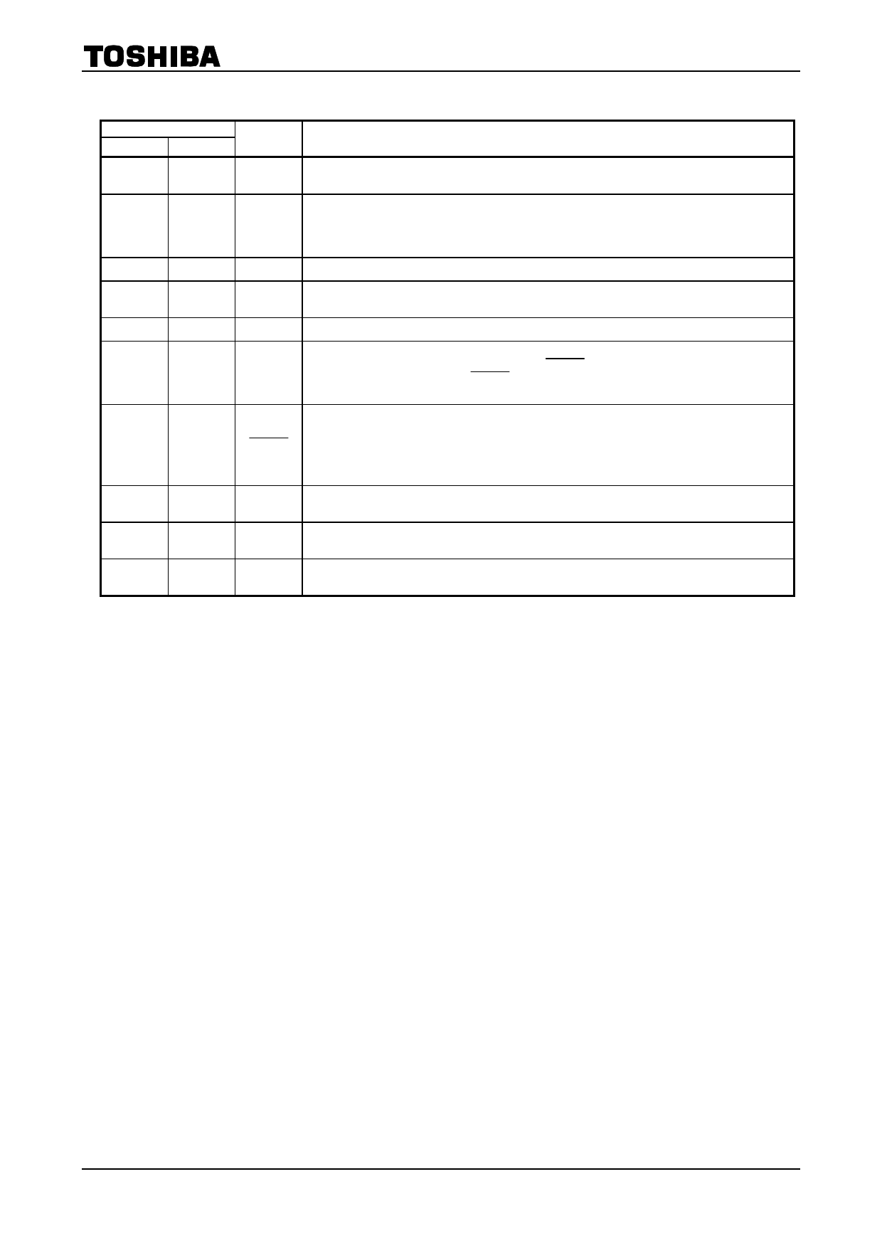
PIN DESCRIPTION
PIN No.
TA8007S TA8007F
1
3
2
4
3
5
4
6
5
8
6
11
7
12
8
13
9
14
―
1, 2, 7, 9,
10, 15, 16
SYMBOL
DESCRIPTION
BIAS
OUT
COMP
VCC
GND
M
RESET
TC
CK
Power supply pin for the start-up circuit which activates the overvoltage detection circuit and
the 5V power supply.
Connected to the base of an external PNP transistor so that the output voltage is stabilized.
Power supply design suitable for particular load capacities is thus possible.
Since the recommended maximum IOUT is 5mA, an output current of 300mA is assured if
the external transistor has an hFE of 60 or more.
Phase compensation pin for output stabilization.
Power supply pin for the power supply section and reset timers. The output voltage VREG
can also be detected at this pin.
Grounded
PN transistor open-collector output
This signal is low while pulses come from RESET pin (output) ; it becomes high when
pulses no longer come from RESET pin. This function can be used for monitoring the
operation of the microcomputer system.
NPN transistor open-collector output.
(1) The signal goes low when the output voltage drops below 92%.
(2) The pin supplies a reset signal determined by the CR combination connected to the TC
pin.
(3) The pin supplies reset pulses intermittently if no clock is given to the CK pin.
Time setting pin for the reset and watchdog timers. The resistor RT leads to VCC, and the
capacitor CT leads to GND.
Input pin for watchdog timer. The pin is pulled up to VCC if the IC is used only as a power-on
reset timer.
NC Not connected. (Electrically, this pin is completely open.)
3
2003-02-28
Share Link: 