TDA3617 Ver la hoja de datos (PDF) - Philips Electronics
Número de pieza
componentes Descripción
Lista de partido
TDA3617 Datasheet PDF : 16 Pages
| |||
Philips Semiconductors
Multiple voltage regulator
Preliminary specification
TDA3617
FUNCTIONAL DESCRIPTION
The TDA3617J is a multiple output voltage regulator with
three independent switchable regulators. When the supply
voltage (VP > 4.5 V) is available, regulators 1, 2 and 3 can
be operated by means of three independent enable inputs.
Schmitt trigger functions are included to switch the
regulators off at low battery voltage (VP < 4 V).
A hysteresis is included to avoid random switching.
All output pins are fully protected. The regulators are
protected against load dump (the regulators switch off at
supply voltages higher than 20 V) and short circuit
(foldback current protection).
The TDA3617J has a hold circuit which indicates when
one of the regulators is out-of-regulation. The hold function
is disabled when all the enable inputs are LOW
(TDA3617J in standby mode). The HOLD output (open
collector output) can be wired OR-ed with other hold
outputs of other regulator parts (e.g. TDA3618). When all
the regulators of the TDA3617J are disabled (switched
off), the HOLD output will be high ohmic. Because of this
feature, the hold will not influence the hold information
when wired OR-ed with other regulator parts.
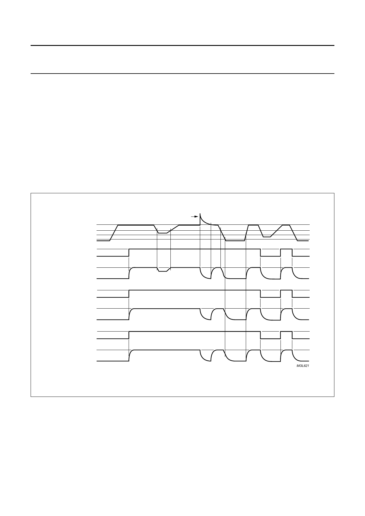
Figure 3 shows the total timing of a semi-on/off logic set.
Figure 4 shows the total timing of the HOLD signal.
handbook, full pagewidth
VP
18.0 V
9.4 V
4.5 V
4.0 V
enable ≥2.2 V
regulator 1 ≤2.0 V
9.0 V
regulator 1
0V
enable ≥2.2 V
regulator 2 ≤2.0 V
5.0 V
regulator 2
0V
enable ≥2.2 V
regulator 3 ≤2.0 V
3.3 V
regulator 3
0V
load dump
Fig.3 Timing diagrams of a semi-on/off logic set.
MGL621
1999 Jul 14
4
Share Link: 