TDA9850 Ver la hoja de datos (PDF) - Philips Electronics
Número de pieza
componentes Descripción
Lista de partido
TDA9850 Datasheet PDF : 32 Pages
| |||
Philips Semiconductors
I2C-bus controlled BTSC stereo/SAP decoder
Preliminary specification
TDA9850
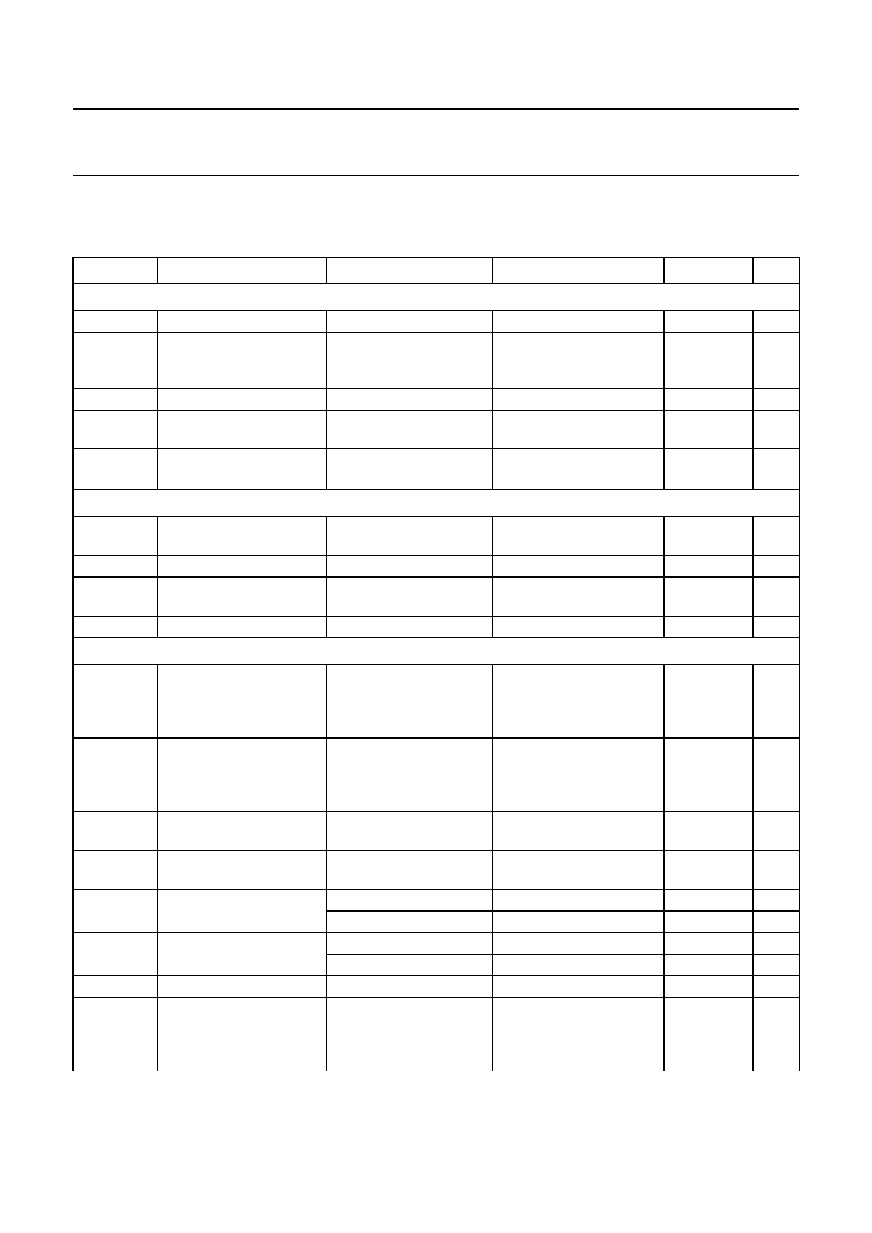
CHARACTERISTICS
All voltages are measured relative to GND; VCC = 9 V; Rs = 600 Ω; RL = 10 kΩ; AC-coupled; CL = 2.5 nF; fi = 1 kHz;
Tamb = +25 °C; see Fig.1; unless otherwise specified.
SYMBOL
PARAMETER
CONDITIONS
MIN.
TYP.
MAX. UNIT
Supply
VCC
supply voltage
8.5
Vripple(p-p) allowed supply voltage fi = 50 Hz to 100 kHz
−
ripple (peak-to-peak
value)
ICC
supply current
−
Vref
internal reference voltage
−
at pin Vref
αct
crosstalk between bus notes 1 and 2
−
inputs and signal outputs
9
9.5
V
−
100
mV
58
75
mA
3.7
−
V
110
−
dB
Input level adjustment control
GLA
input level adjustment
control
−3.5
−
+4.0
dB
Gstep
Vi(rms)
step resolution
maximum input voltage
level (RMS value)
−
0.5
−
dB
2
−
−
V
Zi
input impedance
29.5
35
40.5
kΩ
Stereo decoder
MPXL+R
input voltage level for
input level adjusted via −
250
−
mV
100% modulation L + R; I2C-bus (L + R;
25 kHz deviation
(RMS value)
fi = 300 Hz); monitoring
OUTL or OUTR
MPXL−R
input voltage level for
100% modulation L − R;
50 kHz deviation
(peak value)
−
707
−
mV
MPX(max) maximum headroom for fmod < 15 kHz;
9
−
−
dB
L + R, L, R
THD < 15%
MPXpilot
nominal stereo pilot
voltage level (RMS value)
−
50
−
mV
STon(rms)
pilot threshold voltage
stereo on (RMS value)
data STS = 1
data STS = 0
−
−
35
mV
−
−
30
mV
SToff(rms)
pilot threshold voltage
stereo off (RMS value)
data STS = 1
data STS = 0
15
−
−
mV
10
−
−
mV
Hys
hysteresis
−
2.5
−
dB
OUTL+R
output voltage level for input level adjusted via 480
500
520
mV
100% modulation L + R at I2C-bus (L + R;
OUTL, OUTR
fi = 300 Hz); monitoring
OUTL or OUTR
1995 Jun 19
11
Share Link: 