TGA4508 Ver la hoja de datos (PDF) - TriQuint Semiconductor
Número de pieza
componentes Descripción
Lista de partido
TGA4508 Datasheet PDF : 11 Pages
| |||
TGA4508
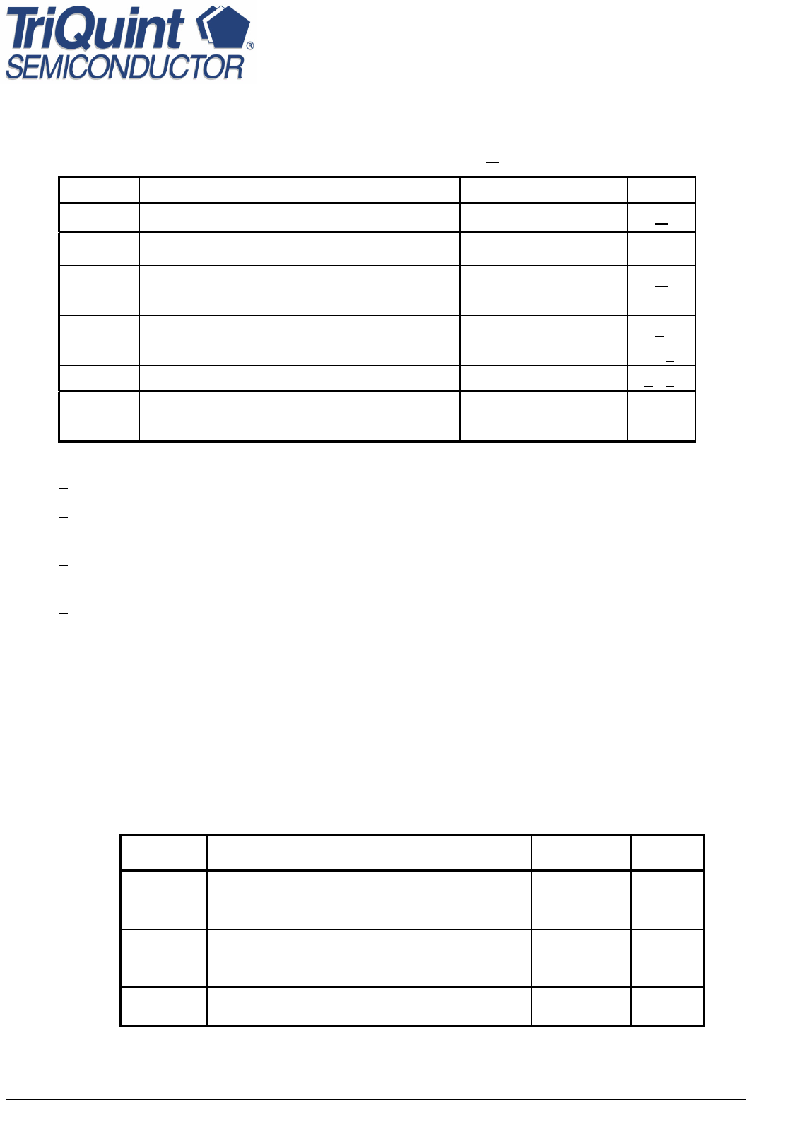
TABLE I
MAXIMUM RATINGS 1/
SYMBOL
PARAMETER
V+
Positive Supply Voltage
Vg1 Gate 1 Supply Voltage Range
I+
Positive Supply Current
| IG | Gate Supply Current
PIN Input Continuous Wave Power
PD Power Dissipation
TCH Operating Channel Temperature
Mounting Temperature (30 Seconds)
TSTG Storage Temperature
VALUE
5V
-1 V TO 0 V
190 mA
6 mA
12 dBm
0.95 W
200 °C
320 °C
-65 to 150 °C
NOTES
2/
2/
2/
2/, 3/
4/, 5/
1/ These ratings represent the maximum operable values for this device.
2/ Current is defined under no RF drive conditions. Combinations of supply voltage, supply
current, input power, and output power shall not exceed PD.
3/ When operated at this power dissipation with a base plate temperature of 70 °C, the median life
is 3.0E3 hours.
4/ Junction operating temperature will directly affect the device median time to failure (Tm). For
maximum life, it is recommended that junction temperatures be maintained at the lowest
possible levels.
5/ These ratings apply to each individual FET.
TABLE II
DC PROBE TESTS
(Ta = 25 °C, Nominal)
SYMBOL
PARAMETER
VBVGS3
Breakdown Voltage gate-
source
VBVGD3
Breakdown Voltage gate-
drain
VP1,2,3
Pinch-off Voltage
MINIMUM MAXIMUM UNITS
-30
-5
V
-30
-5
V
-1.0
-0.1
V
Q1 is 100 um FET, Q2 is 200 um FET, Q3 is 300 um FET
2
TriQuint Semiconductor: www. triquint.com (972)994-8465 Fax (972)994-8504 Info-mmw@tqs.com
May 2009 © Rev -
Share Link: 