TGA4517(2006) Ver la hoja de datos (PDF) - TriQuint Semiconductor
Número de pieza
componentes Descripción
Lista de partido
TGA4517 Datasheet PDF : 10 Pages
| |||
Advance Product Information
February 10, 2006
TGA4517
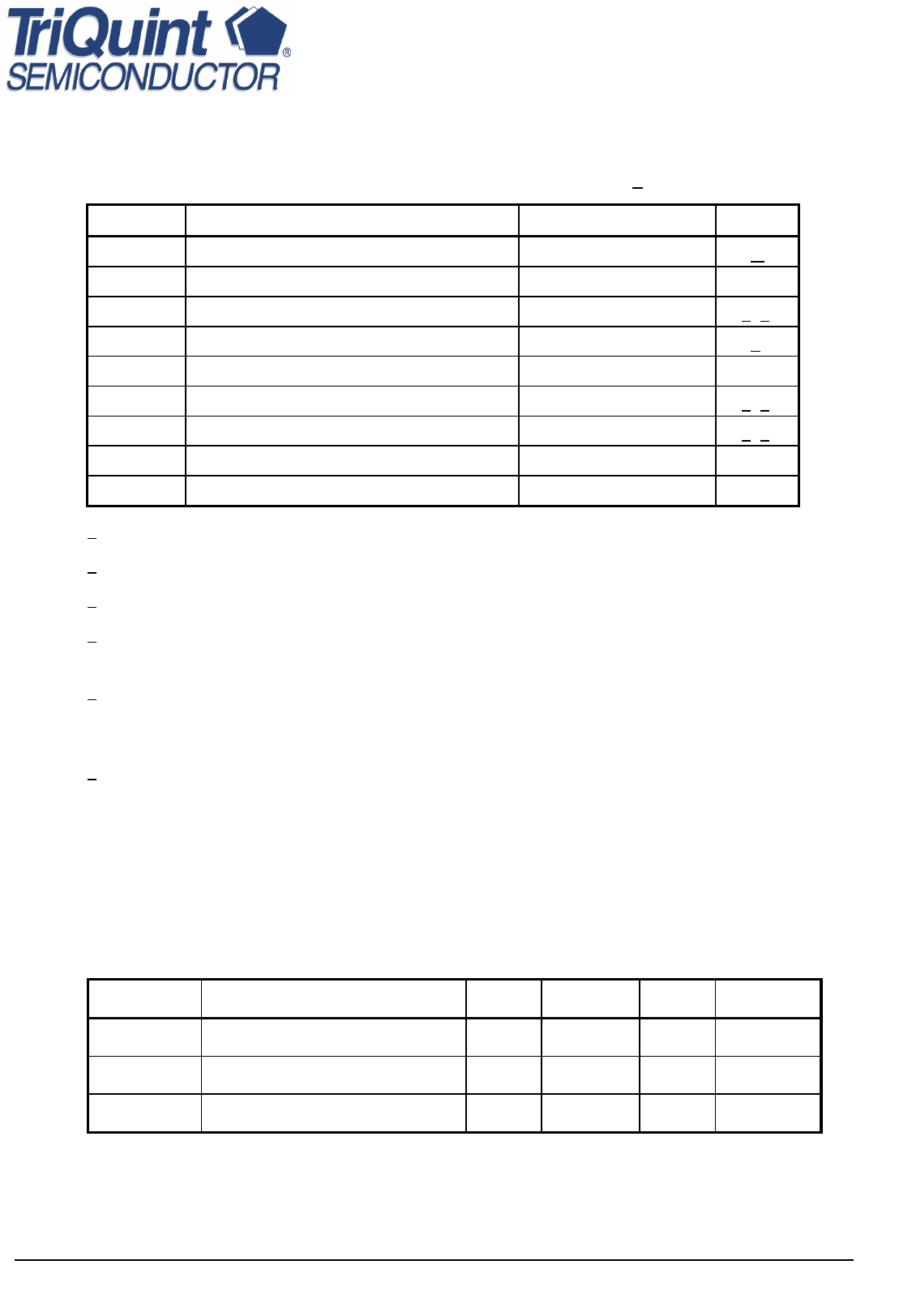
TABLE I
ABSOLUTE MAXIMUM RATINGS 1/
SYMBOL
PARAMETER
VALUE
NOTES
Vd
Vg
Id
Ig
PIN
PD
TCH
TM
TSTG
Drain Voltage
Gate Voltage Range
Drain Current (Under RF Drive)
Gate Current
Input Continuous Wave Power
Power Dissipation
Operating Channel Temperature
Mounting Temperature (30 Seconds)
Storage Temperature
6.5 V
-3 TO 0 V
4A
141 mA
TBD
18.3 W
150 0C
320 0C
-65 to 150 0C
2/
2/ 3/
3/
2/ 4/
5/ 6/
1/ These ratings represent the maximum operable values for this device.
2/ Combinations of supply voltage, supply current, input power, and output power shall not exceed PD.
3/ Total current for the entire MMIC.
4/ When operated at this bias condition (with RF applied) at a base plate temperature of 70 0C, the
median life is 1E+6 hrs.
5/ Junction operating temperature will directly affect the device median time to failure (MTTF). For
maximum life, it is recommended that junction temperatures be maintained at the lowest possible
levels.
6/ These ratings apply to each individual FET.
TABLE II
DC PROBE TESTS
(Ta = 25 0C, Nominal)
SYMBOL
PARAMETER
VBVGD,Q1-Q2 Breakdown Voltage Gate-Drain
VBVGD,Q15-Q30 Breakdown Voltage Gate-Drain
VP,Q15-Q30
Pinch-Off Voltage
Each FET Cell is 750um
MIN.
-30
-30
-1.5
TYP.
-14
-14
-1
MAX.
-11
-11
-0.5
UNITS
V
V
V
TriQuint Semiconductor Texas: Phone (972)994-8465 Fax (972)994-8504 Email: Info-mmw@tqs.com Web: www.triquint.com 2
Share Link: 