MSM82C84A-2GS Ver la hoja de datos (PDF) - Oki Electric Industry
Número de pieza
componentes Descripción
Lista de partido
MSM82C84A-2GS Datasheet PDF : 18 Pages
| |||
¡ Semiconductor
MSM82C84A-2RS/GS/JS
OPERATIONAL DESCRIPTION
(1) Oscillator Circuit
The MSM82C84A-2 internal oscillator circuit can be driven by connecting a crystal oscillator to
the X1 and X2 pins.
The frequency of the crystal oscillator in this case needs to be three times greater than the desired
CLK frequency.
Since the oscillator circuit output (the same output as for the crystal resonator frequency)
appears at the OSC pin, independent use of this output is also possible.
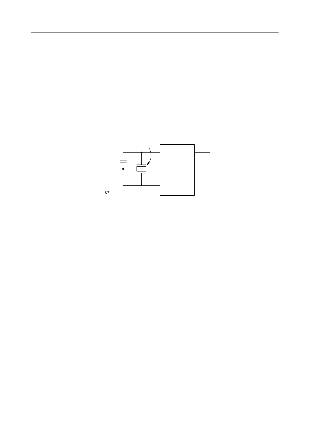
Oscillator Circuit Example
Crystal Oscillator
X1
OSC
C1
MSM
C2
82C84A-2
X2
When input frequency is 6 to 15 MHz
C1 = C2 = 33 pF
When input frequency is 15 to 24 MHz
C1 = C2 = 10 pF
Note: Because Oscillator circuit and values depend on crystal oscillator characteristics,
OKI recommends to make contact with crystal oscillator vendor to determine
the best circuit and values for customers' application.
(2) Clock Generator Circuit
This circuit generates two clock outputs-CLK obtained by dividing the input external clock or
crystal oscillator circuit output by three, and PCLK obtained by halving CLK. CLK and PCLK
are generated from the external clock applied to the EFI pin when F/C is at high level, and are
generated from the crystal oscillator circuit when at low level.
(3) Reset Circuit
Since a Schmitt trigger circuit is used in the RES input, the MSM82C84A-2 can be reset by “power
on” by connection to a simple RC circuit. If the MSM80C86A-10 or MSM80C88A-10 is used as
the CPU in this case, it is necessary to keep the RES input at low level for at least 50 ms after Vcc
reaches the 4.5V level.
9/18
Share Link: 