PI6C110EV Ver la hoja de datos (PDF) - Pericom Semiconductor
Número de pieza
componentes Descripción
Lista de partido
PI6C110EV Datasheet PDF : 15 Pages
| |||
PI6C110E
Clock Solution for 133 MHz
11223344556677889900112233445566778899001122334455667788990011221122334455667788990011223344556677889900112233445566778899001122112233445566778899001122334455667788990011223344556677889900C112211e22l33e44r5566o77n8899/00P1122e33n4455t66i77u88m99001122I33I44/55I66I7788I9900P11r2211o22c3344e55s66s7788o99r00s1122
PI6C110E Conditions
At power up all SDRAM outputs are enabled and active. The SDATA and SCLK inputs have internal pull-up resistors with values
above 100K Ohms as well for complete platform flexibility.
PI6C110E Serial Configuration Map
A) The serial bits will be read by the clock driver in the following order:
Byte 0 - Bits 7, 6, 5, 4, 3, 2, 1, 0
Byte 1 - Bits 7, 6, 5, 4, 3, 2, 1, 0
Byte N - Bits 7, 6, 5, 4, 3, 2, 1, 0
B) All unused register bits (reserved and N/A) are designed as don't care. The controller will force all of these bits to a 0 level.
C) All reserved bits should be programmed to a logic level 0.
Note:
1. Default is for ALL clocks to be enabled and all reserved bits should be programmed to a logic level 0.
Spread spectrum modulation should power up disabled (Byte 0 bit 3 = 0).
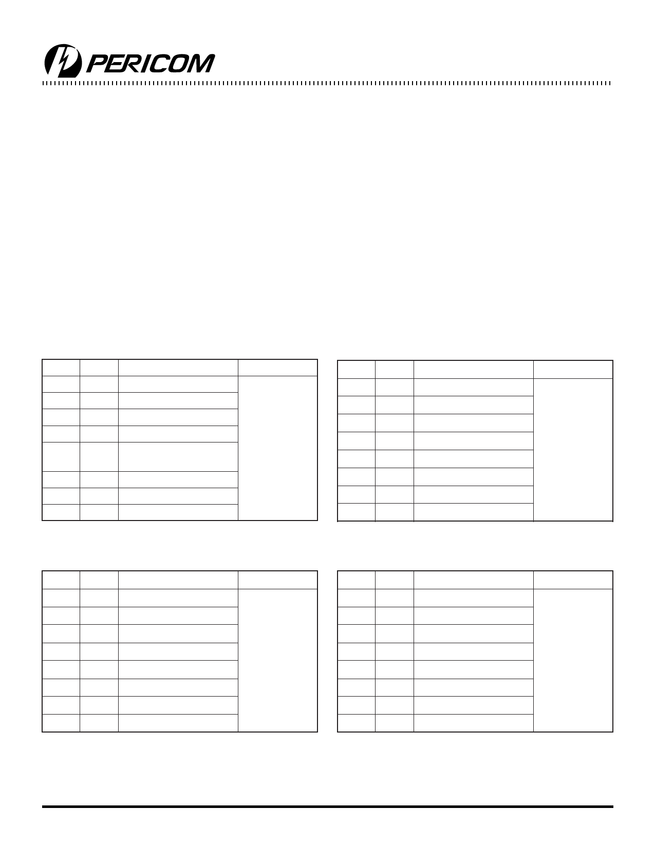
Byte 0 : Control Register (1 = Enable, 0 = Disable)
Bit Pin#
Name
Bit 7 Reserved Drive to '0'
Bit 6 Reserved Drive to '0'
Bit 5 Reserved Drive to '0'
Pin Description
Bit 4 Reserved Drive to '0'
Bit 3
Spread Spectrum
(1 = On / 0 = Off)
Bit 2 26 USB1
Bit 1 25 USB0
Bit 0 49 CPU2
(Active/Inactive)
Byte 1: Control Register (1 = Enable, 0 = Disable)
Bit Pin#
Name
Pin Description
Bit 7 36 SDRAM7
Bit 6 37 SDRAM6
Bit 5 39 SDRAM5
Bit 4 40 SDRAM4
Bit 3 42 SDRAM3
(Active/Inactive)
Bit 2 43 SDRAM2
Bit 1 45 SDRAM1
Bit 0 46 SDRAM0
Byte 2: Control Register (1 = Enable, 0 = Disable)
Bit Pin#
Name
Pin Description
Bit 7 20 PCI7
Bit 6 19 PCI6
Bit 5 18 PCI5
Bit 4 16 PCI4
Bit 3 15 PCI3
(Active/Inactive)
Bit 2 13 PCI2
Bit 1 12 PCI1
Bit 0 Reserved Drive to '0'
Byte 3 and Byte 4:
Reserved Register (1 = Enable, 0 = Disable)
Bit Pin#
Name
Pin Description
Bit 7 Reserved Drive to '0'
Bit 6 Reserved Drive to '0'
Bit 5 Reserved Drive to '0'
Bit 4 Reserved Drive to '0'
Bit 3 Reserved Drive to '0'
(Active/Inactive)
Bit 2 Reserved Drive to '0'
Bit 1 Reserved Drive to '0'
Bit 0 Reserved Drive to '0'
Note: Inactive means outputs are held LOW and are disabled from switching. These outputs are designed to be configured at power-on and are not
expected to be configured during the normal modes of operation.
14
PS8410
08/11/99
Share Link: 