GTLP16612A Ver la hoja de datos (PDF) - Pericom Semiconductor
Número de pieza
componentes Descripción
Lista de partido
GTLP16612A Datasheet PDF : 8 Pages
| |||
GTLP16612A 111222333444555666777888999000111222333444555666777888999000111222333444555666777888999000111222111222333444555666777888999000111222333444555666777888999000111222333444555666777888999000111222111222333444555666777888999000111222333444555666777888999000111222333444555666777888999000111222111222333444555666777888999000111222333444555666777888999000111222333444555666777888999000111222111222333444555666777888999000111222
CMOS 18-Bit TTL/GTLP Universal Bus Transceiver
Features
Bidirectional interface between GTLP and TTL
logic levels
Designed with Edge Rate Control Circuit to
reduce output noise
VREF pin provides external supply reference voltage
for receiver threshold
5V tolerant inputs and outputs on A-Port
Increased B-Port Drive, 50mA
Bus-Hold data inputs on A-Port to eliminate the need for
pull-up resistors for unused inputs
Power up/down high impedance
TTL compatible Driver and Control inputs
A-Port Balanced Drive: 32mA/+32mA
Flow-through architecture
Open drain on GTLP to support wired-or connection
Package:
56-pin 240 Mil Wide Plastic TSSOP (A)
Logic Block Diagram
1
OEAB
CEAB 56
CLKAB 55
LEAB 2
LEBA 28
CLKBA 30
CEBA 29
OEBA 27
A1 3
CE
1D
CI
CLK
1 of 18 Channels
CE
1D
54
CI
GTLP
B1
CLK
1 of 18 Channels
Product Description
Pericom Semiconductors GTLP series of logic circuits are produced
using the Companys advanced 0.5 micron CMOS technology,
achieving industry leading performance.
The GTLP16612A 18-bit universal transceiver provides TTL to GTLP
signal level translation. The device is designed to provide high-
speed interface between cards operating at TTL logic levels and a
back plane operating at GTLP logic levels. High-speed back plane
operation is a direct result of GTLPs reduced output swing (<1V),
reduced input threshold levels, and output edge-rate control which
minimizes signal settling times. Its function is similar to BTL or GTL
but with modified driver output levels and receiver threshold. GTLP
output low voltage is typically less than 0.5V, the output high is 1.5V,
and the receiver threshold is 1.0V.
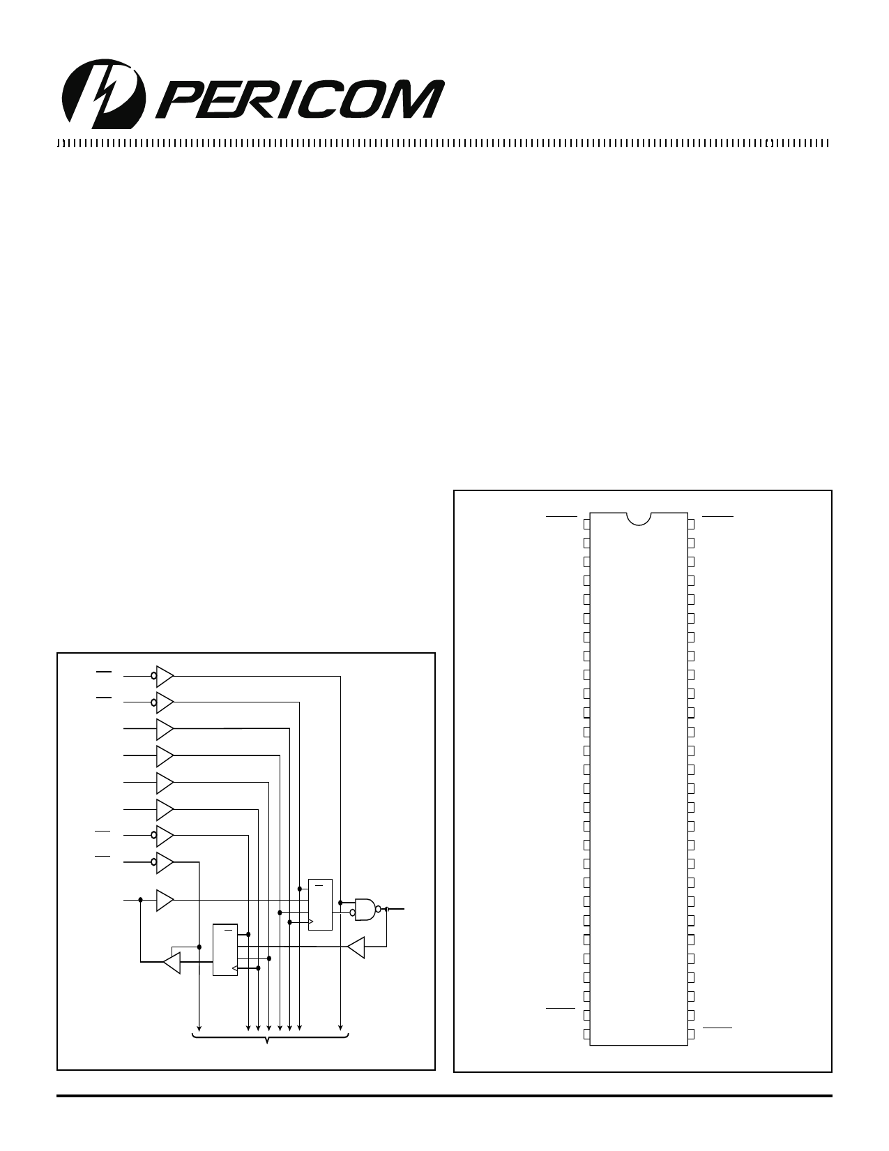
Pin Configuration
OEAB
LEAB
A1
GND
A2
A3
VCC(3.3V)
A4
A5
A6
GND
A7
A8
A9
A10
A11
A12
GND
A13
A14
A15
VCC(3.3V)
A16
A17
GND
A18
OEBA
LEBA
1
56
2
55
3
54
4
53
5
52
6
51
7
50
8
49
9
48
10
47
11
46
12 56-Pin 45
A,V
13
44
14
43
15
42
16
41
17
40
18
39
19
38
20
37
21
36
22
35
23
34
24
33
25
32
26
31
27
30
28
29
CEAB
CLKAB
B1
GND
B2
B3
VCCQ(5.0V)
B4
B5
B6
GND
B7
B8
B9
B10
B11
B12
GND
B13
B14
B15
VREF
B16
B17
GND
B18
CLKBA
CEBA
1
PS8431 09/24/99
Share Link: 