UBA1707 Ver la hoja de datos (PDF) - Philips Electronics
Número de pieza
componentes Descripción
Lista de partido
UBA1707 Datasheet PDF : 36 Pages
| |||
Philips Semiconductors
Cordless telephone, answering machine
line interface
Product specification
UBA1707
FUNCTIONAL DESCRIPTION
All data given in this chapter are typical values, except
when otherwise specified.
Supply (pins VCC and GND; bits PD and LSPD)
The UBA1707 must be supplied with an external stabilized
voltage source between pins VCC and GND.
Pins GND and LSPGND must be connected together.
Without any signal, with the loudspeaker channel enabled
at minimum volume and without any general purpose
switch selected, the internal current consumption is
2.2 mA at VCC = 3.3 V. Each selected switch
(pins SWI1, SWI2, or SWI3) increases the current
consumption by 600 µA.
The supply current can be reduced when the loudspeaker
channel is not used by switching it off (bit LSPD at logic 1).
The current consumption is then decreased by
approximately 800 µA at minimum volume.
To drastically reduce current consumption, the UBA1707
is provided with a power-down mode controlled by bit PD.
When bit PD is at logic 1, the current consumption from
VCC becomes 110 µA. In this mode, the serial interface is
the only function which remains active.
Line interface
DC CHARACTERISTICS (PINS LN, SLPE, REG, CST, LVI,
LCC, RGL AND GND; BIT CRC)
The IC generates a stabilized reference voltage (Vref)
between pins LN and SLPE. This reference voltage is
equal to 2.9 V, is temperature compensated and can be
adjusted by means of an external resistor (RVA). It can be
increased by connecting the RVA resistor between
pins REG and SLPE (see Fig.3).
The voltage at pin REG is used by the internal regulator to
generate the stabilized reference voltage and is decoupled
by a capacitor (CREG) which is connected to GND. This
capacitor, converted into an equivalent inductance
(see Section “Set impedance”) realizes the set impedance
conversion from its DC value (RSLPE) to its AC value
(ZSET in the audio-frequency range). Figure 4 illustrates
the reference voltage supply configuration. As can be seen
from Fig.4, part of the line current flows into the ZSET
impedance network and is not sensed by the UBA1707.
Therefore using the RVA resistor to change value of the
reference voltage will also modify all parameters related to
the line current such as:
• The automatic gain control
• The DC mask management
• The low voltage area characteristics.
In the same way, changing the value of ZSET also affects
the characteristics. The IC has been optimized for
Vref = 2.9 V and ZSET = 619 Ω.
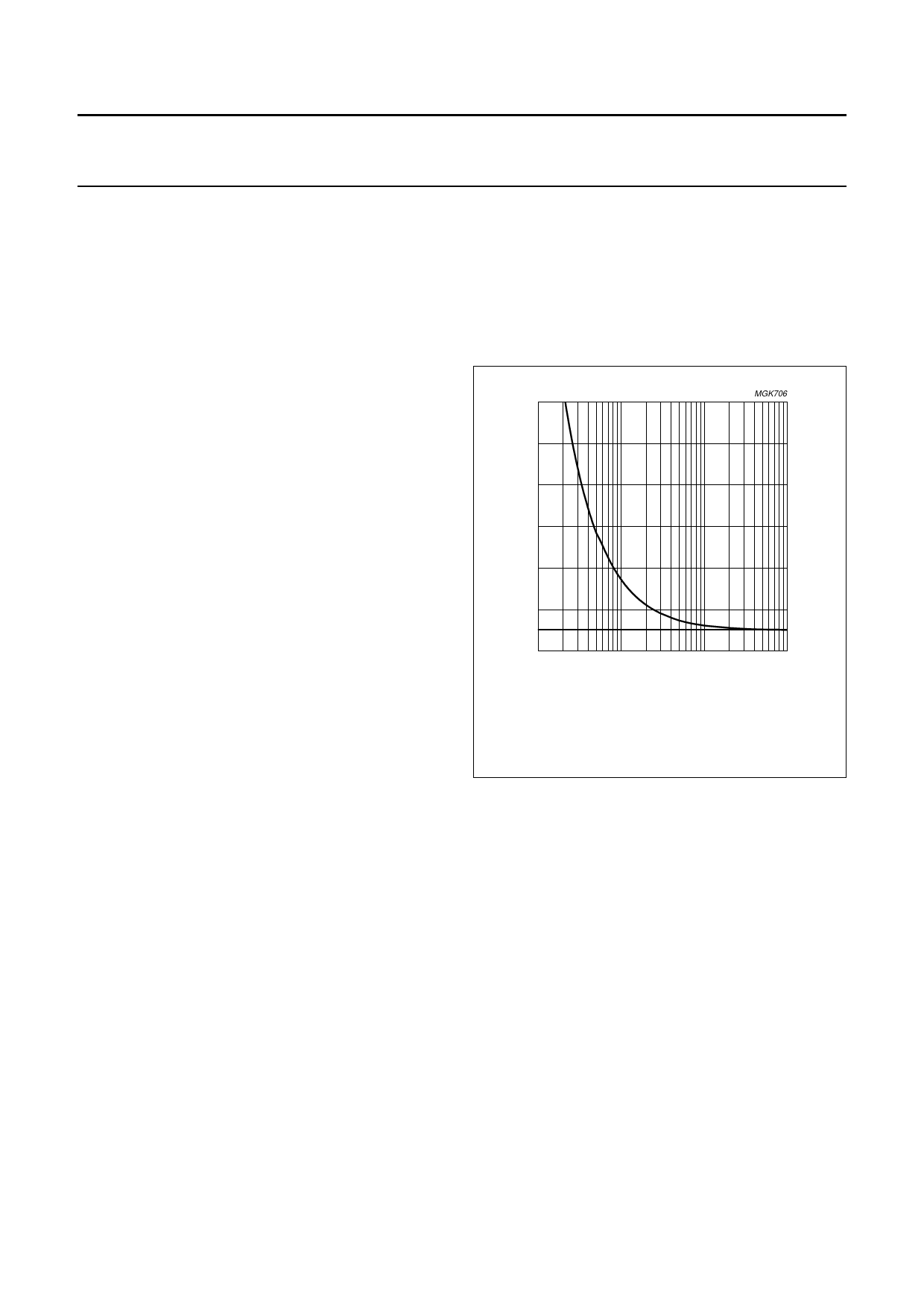
8.5
handVboreokf, halfpage
(V)
7.5
MGK706
6.5
5.5
4.5
(1)
3.5
(2)
2.5
103
104
105 RVA (Ω) 106
(1) Influence of RVA on Vref.
(2) Vref without influence of RVA.
Fig.3 Reference voltage adjustment with RVA.
The IC regulates the line voltage at pin LN which can be
calculated as follows:
VLN = Vref + RSLPE × ISLPE
ISLPE = Iline – IZSET – I* ≅ Iline – IZSET
Where:
Iline = line current
IZSET = current flowing through ZSET
I* = current consumed between LN and GND
(approximately 100 µA).
The preferred value for RSLPE is 10 Ω. Changing RSLPE will
affect more than the DC characteristics; it also influences
the transmit gain, the gain control characteristics, the
sidetone level and the maximum output swing on the line.
However, for compliance with CTR 21 8.66 Ω is the best
value for RSLPE.
1999 Feb 17
6
Share Link: 