IR2125(Old_V) Ver la hoja de datos (PDF) - International Rectifier
Número de pieza
componentes Descripción
Lista de partido
IR2125 Datasheet PDF : 16 Pages
| |||
Previous Datasheet
Index
Next Data Sheet
IR2125
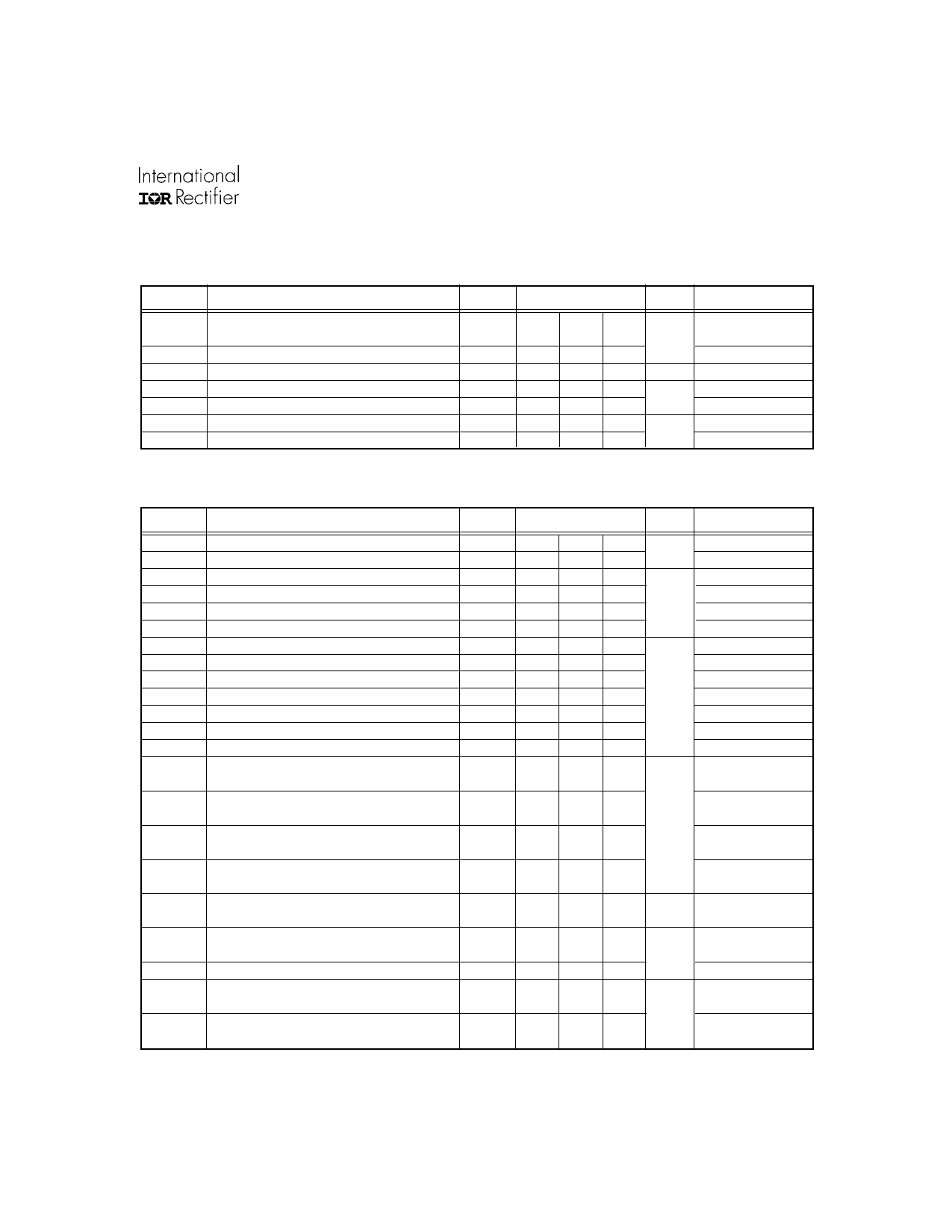
Dynamic Electrical Characteristics
VBIAS (VCC, VBS) = 15V, CL = 3300 pF and TA = 25°C unless otherwise specified. The dynamic electrical characteristics
are measured using the test circuit shown in Figures 3 through 6.
Parameter
Value
Symbol
Definition
Figure Min. Typ. Max. Units Test Conditions
ton
Turn-On Propagation Delay
toff
Turn-Off Propagation Delay
tsd
ERR Shutdown Propagation Delay
tr
Turn-On Rise Time
tf
Turn-Off Fall Time
tcs
CS Shutdown Propagation Delay
terr
CS to ERR Pull-Up Propagation Delay
7
—
150 200
ns
8
— 150 190
9
— 1.7 2.2 µs
10
—
43 60
ns
11
— 26 35
12
—
0.7 1.2
µs
13
— 9.0 12
CERR = 270 pF
Static Electrical Characteristics
VBIAS (VCC, VBS) = 15V and TA = 25°C unless otherwise specified. The VIN, VTH and IIN parameters are referenced to
COM. The VO and IO parameters are referenced to VS.
Symbol
VIH
VIL
VCSTH+
VCSTH-
VOH
VOL
ILK
IQBS
IQCC
IIN+
IIN-
ICS+
ICS-
VBSUV+
VBSUV-
VCCUV+
VCCUV-
IERR
IERR+
IERR-
IO+
IO-
Parameter
Definition
Logic “1” Input Voltage
Logic “0” Input Voltage
CS Input Positive Going Threshold
CS Input Negative Going Threshold
High Level Output Voltage, VBIAS - VO
Low Level Output Voltage, VO
Offset Supply Leakage Current
Quiescent VBS Supply Current
Quiescent VCC Supply Current
Logic “1” Input Bias Current
Logic “0” Input Bias Current
“High” CS Bias Current
“Low” CS Bias Current
VBS Supply Undervoltage Positive Going
Threshold
VBS Supply Undervoltage Negative Going
Threshold
VCC Supply Undervoltage Positive Going
Threshold
VCC Supply Undervoltage Negative Going
Threshold
ERR Timing Charge Current
ERR Pull-Up Current
ERR Pull-Down Current
Output High Short Circuit Pulsed Current
Output Low Short Circuit Pulsed Current
To Order
Value
Figure Min. Typ. Max. Units Test Conditions
14
2.2 —
—
V
VCC = 12V to 18V
15
—
— 0.8
VCC = 12V to 18V
16 150 230 320
VCC = 12V to 18V
17
130 200 260 mV VCC = 12V to 18V
18
—
— 100
IO = 0A
19
—
— 100
IO = 0A
20
—
—
50
VB = VS = 500V
21
— 400 1000
VIN = VCS = 0V or 5V
22
— 700 1200
VIN = VCS = 0V or 5V
23
— 4.5 10 µA
VIN = 5V
24
—
— 1.0
VIN = 0V
25
— 4.5 10
VCS = 3V
26
—
— 1.0
VCS = 0V
27
8.5 9.2 10.0
28
7.7 8.3 9.0
V
29
8.3 8.9 9.6
30
7.3 8.0 8.7
31
65
100 130 µA VIN = 5V, VCS = 3V
ERR < VERR+
32
8.0 15 —
VIN = 5V, VCS = 3V
mA
ERR > VERR+
33
16 30 —
VIN = 0V
34
1.0 1.6 —
VO = 0V, VIN = 5V
PW ≤ 10 µs
A
35
2.0 3.3 —
VO = 15V, VIN = 0V
PW ≤ 10 µs
CONTROL INTEGRATED CIRCUIT DESIGNERS MANUAL B-109
Share Link: 