Z9975 Ver la hoja de datos (PDF) - Cypress Semiconductor
Número de pieza
componentes Descripción
Lista de partido
Z9975 Datasheet PDF : 8 Pages
| |||
Z9975
3.3V, 150MHz, Multi-Output Zero Delay Buffer
AC Parameters
Characteristic
Symbol
Min
Typ
Max Units Conditions
Output Duty Cycle
Tpw Tcycle/2 Tcycle/2 Tcycle/2 ps Measured @ VDD/2
- 800 + 500 + 800
Rise Time / Fall Time
Output Impedance
Output to Output Skew
Propagation Delay,
TCLK(0:1) to FBIN
Tr, Tf
0.15
-
1.5
ns Measured between 0.8V and 2.0V
Zo
7
10
Ω
Ts
-
-
250
ps All output equally loaded
Tpd
-250
-
100
ps Measured for 50MHz at VDD/2
Cycle to Cycle Jitter
tj
-
+100
-
ps Measured for 50 MHz at VDD/2
Output Disable Time
tPLZ,
2
tPHZ
-
10
ns After MR# goes low
Output Enable Time
tPZL
2
-
10
ns After MR# goes High
Maximum Output
Frequency
Fout
-
-
-
150 MHz Q (÷2)
-
125
Q (÷4)
-
-
83
Q (÷6)
VDD* = 3.3V + 5%, TA = -40°C to +85°C
Note: Parameters are guaranteed by design and characterization. Not 100% tested in production. All parameters
specified with loaded outputs. Z9975 outputs can drive series or parallel terminator 50 Ω (or 50 Ω to VDD/2).
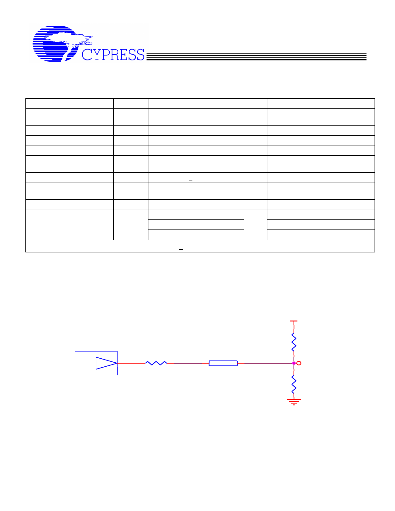
Test Circuit Diagram
Output under Test
7Ω
43 Ω
50 Ω Impedance
VDD*
1K Ω
PROBE
1KΩ
NOTE: All buffer outputs are tied to a common 3.3 Volt
VDD (VDD*) for testing purposes
Cypress Semiconductor Corporation
http://www.cypress.com
Document#: 38-07091 Rev. *B
12/26/2002
Page 6 of 8
Share Link: 