L4904A Ver la hoja de datos (PDF) - STMicroelectronics
Número de pieza
componentes Descripción
Lista de partido
L4904A Datasheet PDF : 9 Pages
| |||
L4904A
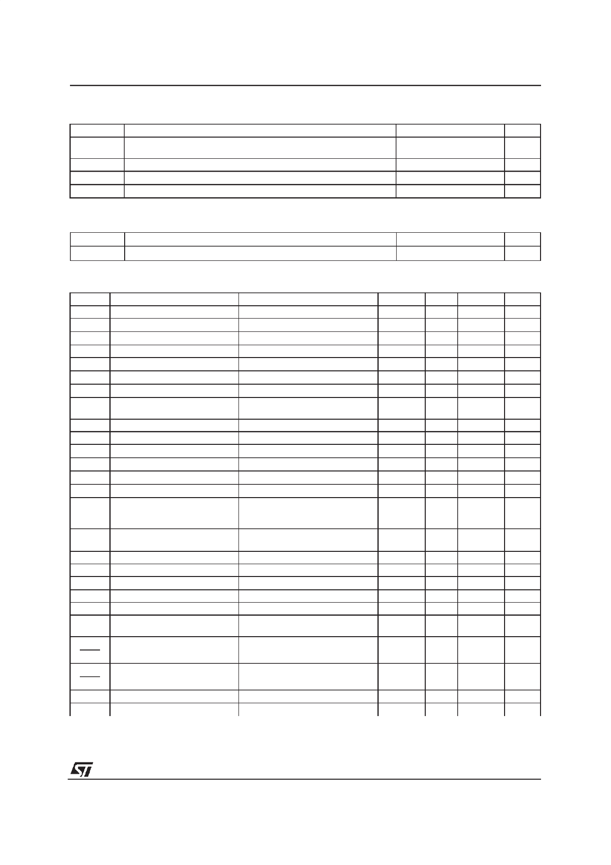
ABSOLUTE MAXIMUM RATINGS
Symbol
VIN
Io
Ptot
Tj
Parameter
DC Input Voltage
Transient Input Overvoltage (t = 40ms)
Output Current
Power Dissipation at Tamb = 50°C
Storage and Junction Temperature
Value
Unit
24
V
60
V
Internally Limited
1
W
– 40 to 150
°C
THERMAL DATA
Symbol
Rth j-amb
Parameter
Thermal Resistance Junction-ambient
Value
Unit
Max
100
°C/W
ELECTRICAL CHARACTERISTICS (VIN = 14.4V, Tamb = 25oC unless otherwise specified)
Symbol
Vi
V01
V02 H
V02 L
I01
IL 01
I02
VI01
Parameter
DC Operating Input Voltage
Output Voltage 1
Output Voltage 2 HIGH
Output Voltage 2 LOW
Output Current 1
Leakage Output 1 Current
Output Current 2
Output 1 Dropout Voltage (*)
VIT
VITH
∆V01
∆V02
∆V01
∆V02
IQ
Input Threshold Voltage
Input Threshold Voltage Hyst.
Line Regulation
Line Regulation 2
Load Regulation 1
Load Regulation 2
Quiescent Current
IQ1 Quiescent Current 1
VRT
VRTH
VRH
VRL
tRD
td
∆V01
∆T
∆V02
∆T
SVR1
SVR2
Reset Threshold Voltage
Reset Threshold Hysteresis
Reset Output Voltage HIGH
Reset Output Voltage LOW
Reset Pulse Delay
Timing Capacitor Discharge
Time
Thermal Drift
Thermal Drift
Supply Voltage Rejection
Supply Voltage Rejection
Test Conditions
R Load 1kΩ
R Load 1kΩ
I02 = – 5mA
∆V01 = – 100mV
VIN = 0, V01 ≤ 3V
∆V02 = – 100mV
I01 = 10mA
I01 = 50mA
7V < VIN < 18V, I01 = 5mA
7V < VIN < 18V, I02 = 5mA
VIN = 8V, 5mA < I01 < 50mA
VIN = 8V, 5mA < I02 < 100mA
I02 = I01 ≤ 5mA
0 < VIN < 13V
7V < VIN < 13V
6.3V < VIN1 < 13V, VIN2 = 0
I01 ≤ 5mA, I02 = 0
IR = 500µA
IR = – 5mA
Ct = 10nF
Ct = 10nF
Min.
4.95
V01 –0.1
50
100
V01 + 1.2
V02 –0.15
30
V02 – 1
3
– 20°C ≤<0>Tamb ≤ 125°C
– 20°C ≤<0>Tamb ≤ 125°C
f = 100Hz, VR = 0.5V, Io = 50mA
50
f = 100Hz, VR = 0.5V, Io = 100mA
50
Typ. Max.
Unit
20
V
5.05 5.15
V
5
V01
V
0.1
V
mA
1
µA
mA
0.7
0.8
V
0.75
0.9
V
6.4 V01 + 1.7 V
250
mV
5
50
mV
5
50
mV
5
20
mV
10
50
mV
mA
4.5
6.5
1.6
3.5
0.6
0.9
mA
4.9 V02 – 0.05 V
50
80
mV
4.12
V02
V
0.25
0.4
V
11
ms
20
µs
0.3
–0.8
0.3
– 0.8
84
80
mV/°C
mV/°C
dB
dB
* The dropout voltage is defined as the difference between the input and the output voltage when the output voltage is lowered of 25 mV under
constant output current condition.
3/9
Share Link: 