ADL5390-EVAL Ver la hoja de datos (PDF) - Analog Devices
Número de pieza
componentes Descripción
Lista de partido
ADL5390-EVAL Datasheet PDF : 24 Pages
| |||
ADL5390
APPLICATIONS
USING THE ADL5390
The ADL5390 is designed to operate in a 50 Ω impedance system.
Figure 29 illustrates an example where the RF/IF inputs are
driven in a single-ended fashion, while the differential RF out-
put is converted to a single-ended output with a RF balun. The
baseband gain controls for the I and Q channels are typically
driven from differential DAC outputs. The power supplies,
VPRF and VPS2, should be bypassed appropriately with 0.1 µF
and 100 pF capacitors. Low inductance grounding of the CMOP
and CMRF common pins is essential to prevent unintentional
peaking of the gain. The exposed paddle on the underside of the
package should be soldered to a low thermal and electrical
impedance ground plane.
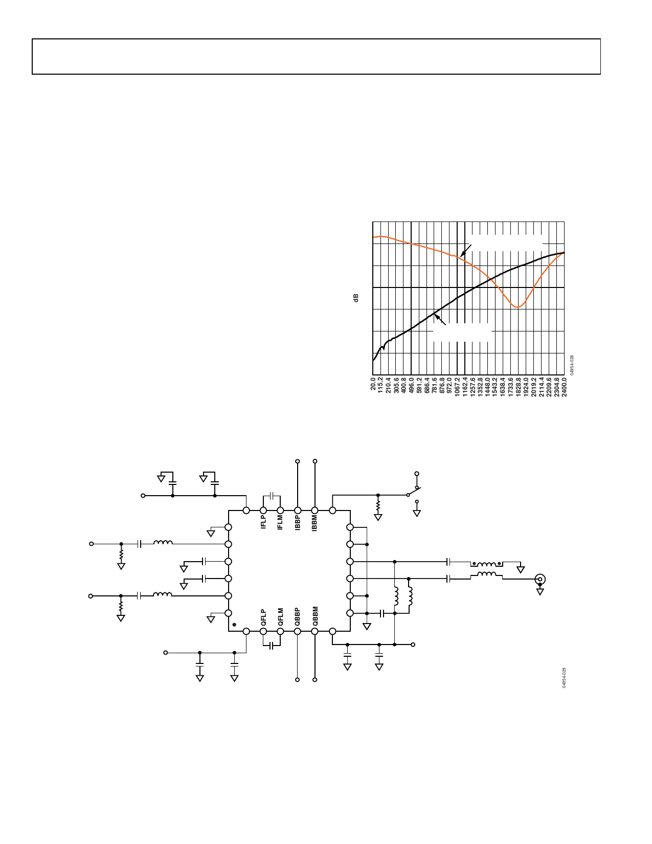
RF INPUT AND MATCHING
The RF/IF inputs present 250 Ω resistive terminations to
ground. In general, the input signals should be ac-coupled
through dc-blocking capacitors. The inputs may be driven dif-
ferentially or single-ended, in which case the unused inputs are
connected to common via the dc-blocking capacitors. The
ADL5390’s performance is not degraded by driving these inputs
single-ended. The input impedance can be reduced by placing
external shunt termination resistors to common on the source
side of the dc-blocking capacitors so that the quiescent dc-bias
level of the ADL5390 inputs is not affected, as shown in Figure
29. Capacitive reactance at the RF inputs can be compensated
for with series inductance. In fact, the customer evaluation
board has high impedance line traces between the shunt termi-
nation pads and the device input pins, which provides series in-
ductance and improves the return loss at 1.9 GHz to better than
−15 dB with the shunt termination removed, as shown in Figure
28.
0
–5
S11 MATCH WITHOUT
66.5Ω TERMINATION
–10
–15
–20
–25
S11 MATCH WITH
TERMINATION
–30
–35
FREQUENCY (MHz)
Figure 28. ADL5390 Customer Evaluation Board RF Input Return Loss.
RFIN_I
RFIN_Q
R2
66.5Ω
R22
66.5Ω
IBBP IBBM
C7
C8
C12
0.1µF
100pF (SEE TEXT)
VP
L1
0Ω
C2
10nF
L2
0Ω
C5
10nF
VPRF
CMRF
C1
10nF
C6
10nF
INPI
INMI
IPMQ
INPQ
CMRF
VPRF
ADL5390
DSOP
CMOP
CMOP
RFOM
RFOP
CMOP
CMOP
VPS2
VP
C4
C3
0.1µF 100pF
C11
(SEE TEXT)
C10
100pF
VP
SW1 B
R8
A
10kΩ
C18
10nF
L4
120nH
C14
0.1µF
C9
0.1µF
C17
L3
10nF
120nH
VP
15
3 T1 4
ETC1-1-13
(M/A-COM)
QBBP QBBM
Figure 29. Basic Connections
RFOP
Rev. 0 | Page 12 of 24
Share Link: 