ADL5390-EVAL Ver la hoja de datos (PDF) - Analog Devices
Número de pieza
componentes Descripción
Lista de partido
ADL5390-EVAL Datasheet PDF : 24 Pages
| |||
ADL5390
The 3 dB bandwidth is set by choosing CFLT according to the
following equation:
45 kHz × 10 nF
f 3 dB ≈ C external + 0.5 pF
This equation has been verified for values of CFLT from 10 pF to
0.1 µF (bandwidth settings of approximately 4.5 kHz to 43 MHz).
INTERFACING TO HIGH SPEED DACs
The AD977x family of dual DACs is well suited to driving the I
and Q gain controls of the ADL5390 with fast modulating sig-
nals. While these inputs can in general be driven by any DAC,
the differential outputs and bias level of the ADI TxDAC® fam-
ily allows for a direct connection between DAC and modulator.
The AD977x family of dual DACs has differential current out-
puts. The full-scale current is user programmable and is usually
set to 20 mA, that is each output swings from 0 mA to 20 mA.
The basic interface between the AD9777 DAC outputs and the
ADL5390 I and Q gain control inputs is shown in Figure 32.
Resistors R1 and R2 (R1 = R2) set the dc bias level according to
the following equation:
Bias Level = Average Output Current × R1
For example, if the full-scale current from each output is 20 mA,
each output will have an average current of 10 mA. Therefore,
to set the bias level to the recommended 0.5 V, R1 and R2
should be set to 50 Ω each. R1 and R2 should always be equal.
If R3 is omitted, this will result in an available swing from the
DAC of 2 V p-p differential, which is twice the maximum voltage
range required by the ADL5390. DAC resolution can be maxi-
mized by adding R3, which scales down this voltage according
to the following equation:
Full Scale Swing =
( ( )) 2× I MAX R1|| R2 + R3
×
⎡
⎢1 −
⎢⎣
R2
R2 + R3
⎤
⎥
⎥⎦
AD9777
IOUTA1
R1
R2
IOUTB1
ADL5390
OPTIONAL
LOW-PASS
FILTER
IBBP
R3
IBBM
IOUTA2
R1
R2
IOUTB2
OPTIONAL
LOW-PASS
FILTER
QBBP
R3
QBBM
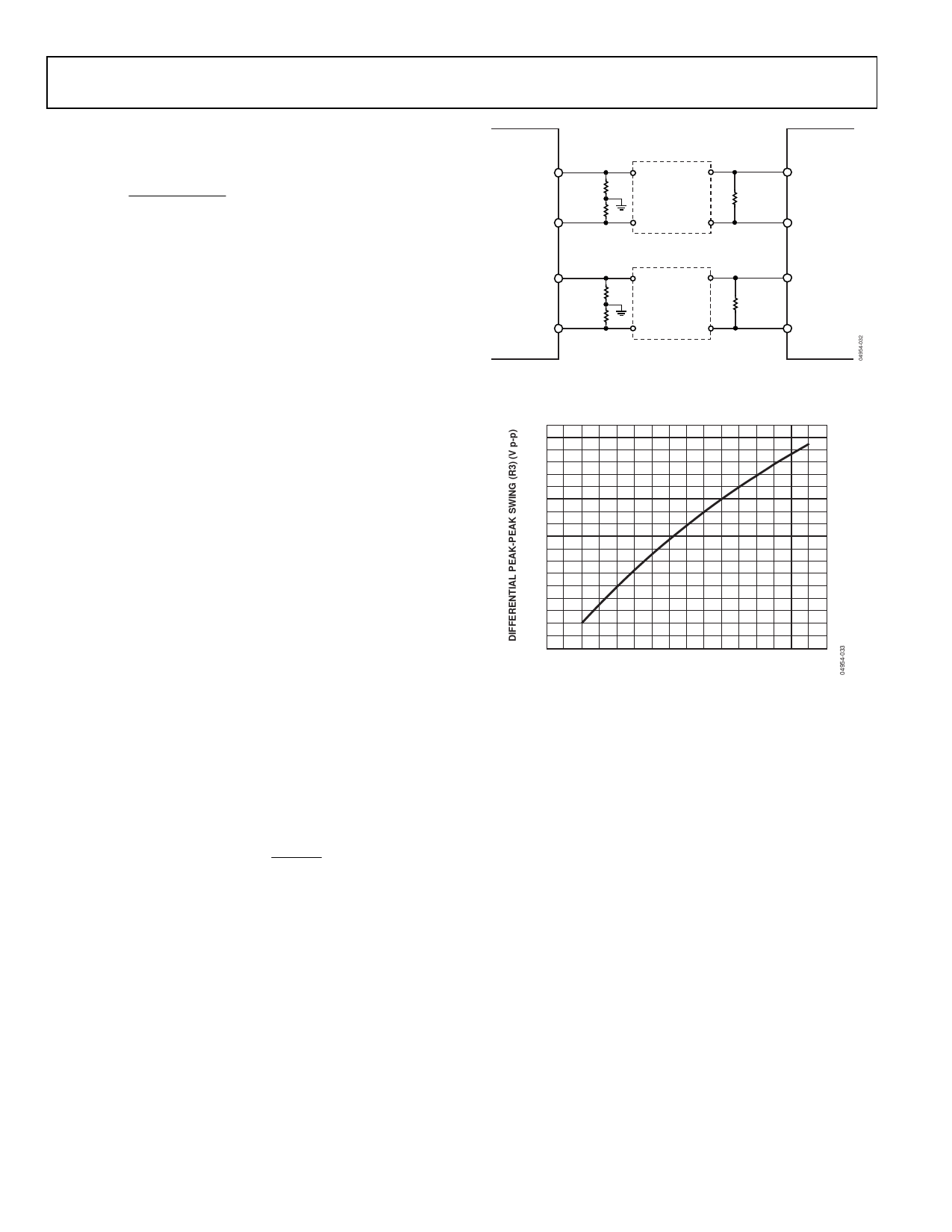
Figure 32. Basic AD9777-to-ADL5390 Interface
1.15
1.13
1.10
1.08
1.05
1.02
1.00
0.97
0.95
0.92
0.90
0.88
0.85
0.82
0.80
0.77
0.75
0.72
0.70
50 55 60 65 70 75 80 85 90 95 100 105 110 115 120 125 130
R3 (Ω)
Figure 33. Peak-Peak DAC Output Swing vs.
Swing Scaling Resistor R3 (R1 = R2 = 50 Ω)
Figure 33 shows the relationship between the value of R3 and
the peak baseband voltage with R1 and R2 equal to 50 Ω. As
shown in Figure 33, a value of 100 Ω for R3 will provide a
peak-peak swing of 1 V p-p differential into the ADL5390’s
I and Q inputs.
When using a DAC, low-pass image reject filters are typically
used to eliminate the Nyquist images produced by the DAC.
They also provide the added benefit of eliminating broadband
noise that might feed into the modulator from the DAC.
Rev. 0 | Page 14 of 24
Share Link: 