ADL5390ACPZ-WP Ver la hoja de datos (PDF) - Analog Devices
Número de pieza
componentes Descripción
Lista de partido
ADL5390ACPZ-WP Datasheet PDF : 24 Pages
| |||
FEATURES
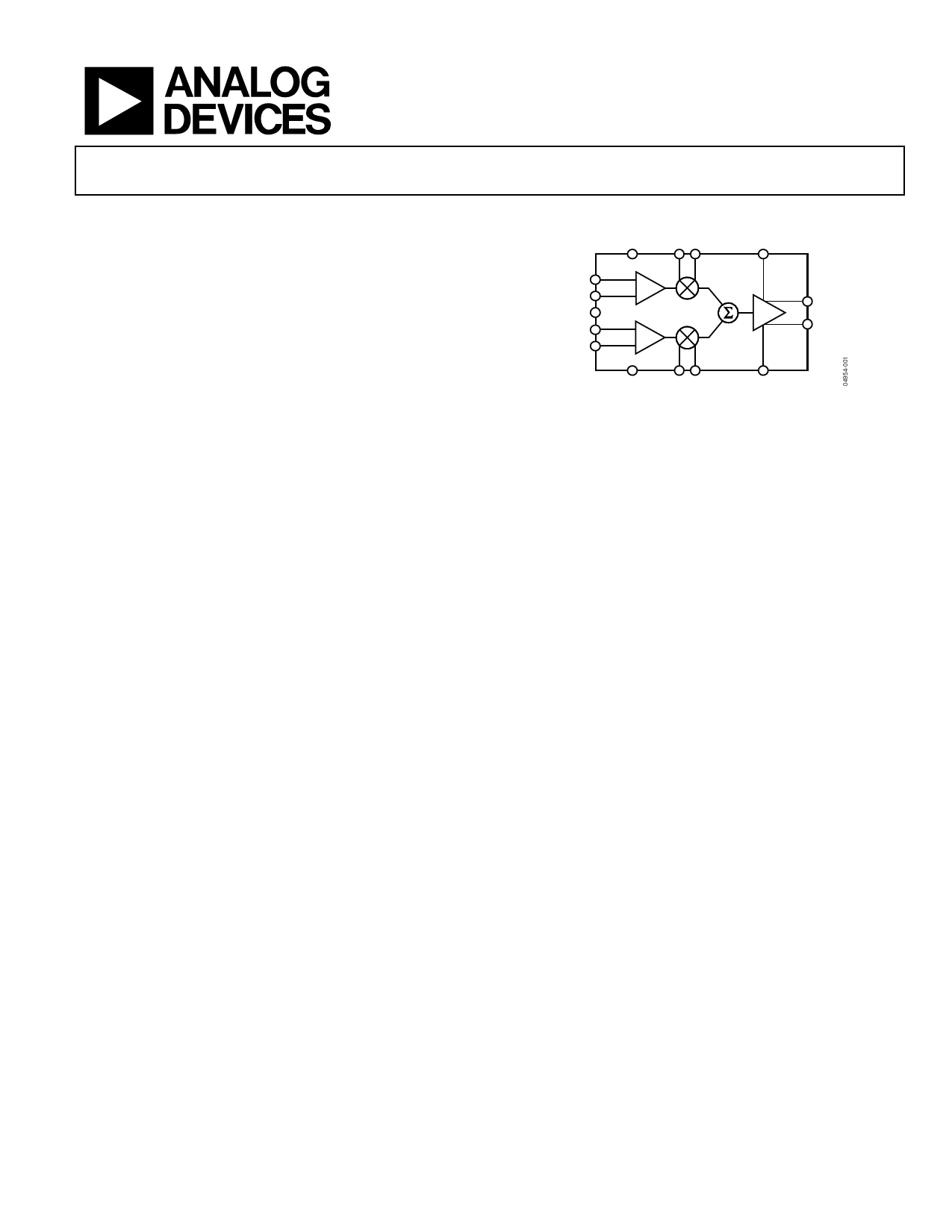
Matched pair of multiplying VGAs
Broad frequency range 20 MHz to 2.4 GHz
Continuous magnitude control from +5 dB to −30 dB
Output third-order intercept 24 dBm
Output 1 dB compression point 11 dBm
Output noise floor −148 dBm/Hz
Adjustable modulation bandwidth up to 230 MHz
Fast output power disable
Single-supply voltage 4.75 V to 5.25 V
APPLICATIONS
PA linearization and predistortion
Amplitude and phase modulation
Variable matched attenuator and/or phase shifter
Cellular base stations
Radio links
Fixed wireless access
Broadband/CATV
RF/IF analog multiplexer
GENERAL DESCRIPTION
The ADL5390 vector multiplier consists of a matched pair of
broadband variable gain amplifiers whose outputs are summed.
The separate gain controls for each amplifier are linear-in-
magnitude. If the two input RF signals are in quadrature, the
vector multiplier can be configured as a vector modulator or as
a variable attenuator/phase shifter by using the gain control pins
as Cartesian variables. In this case, the output amplitude can be
controlled from a maximum of +5 dB to less than –30 dB, and
the phase can be shifted continuously over the entire 360°
range. Since the signal paths are linear, the original modulation
on the inputs is preserved. If the two signals are independent,
then the vector multiplier can function as a 2:1 multiplexer or
can provide fading from one channel to another.
The ADL5390 operates over a wide frequency range of 20 MHz
to 2400 MHz. For a maximum gain setting on one channel at
380 MHz, the ADL5390 delivers an OP1dB of 11 dBm, an OIP3
of 24 dBm, and an output noise floor of −148 dBm/Hz. The gain
and phase matching between the two VGAs is better than 0.5 dB
and 1°, respectively, over most of the operating range.
RF/IF Vector Multiplier
ADL5390
FUNCTIONAL BLOCK DIAGRAM
VPRF QBBP OBBM
VPS2
INMQ
INPQ
CMRF
INPI
INMI
RFOP
RFOM
CMOP IBBP IBBM
DSOP
Figure 1.
The gain control inputs are dc-coupled with a +/−500 mV dif-
ferential full-scale range centered about a 500 mV common
mode. The maximum modulation bandwidth is 230 MHz,
which can be reduced by adding external capacitors to limit the
noise bandwidth on the control lines.
Both the RF inputs and outputs can be used differentially or
single-ended and must be ac-coupled. The impedance of each
VGA RF input is 250 Ω to ground, and the differential output
impedance is nominally 50 Ω over the operating frequency
range. The DSOP pin allows the output stage to be disabled
quickly to protect subsequent stages from overdrive. The
ADL5390 operates off supply voltages from 4.75 V to 5.25 V
while consuming 135 mA.
The ADL5390 is fabricated on Analog Devices’ proprietary,
high performance 25 GHz SOI complementary bipolar IC
process. It is available in a 24-lead, Pb-free CSP package and
operates over a −40°C to +85°C temperature range. Evaluation
boards are available.
Rev. 0
Information furnished by Analog Devices is believed to be accurate and reliable.
However, no responsibility is assumed by Analog Devices for its use, nor for any
infringements of patents or other rights of third parties that may result from its use.
Specifications subject to change without notice. No license is granted by implication
or otherwise under any patent or patent rights of Analog Devices. Trademarks and
registered trademarks are the property of their respective owners.
One Technology Way, P.O. Box 9106, Norwood, MA 02062-9106, U.S.A.
Tel: 781.329.4700
www.analog.com
Fax: 781.326.8703 © 2004 Analog Devices, Inc. All rights reserved.
Share Link: 