ADL5390ACPZ-WP Ver la hoja de datos (PDF) - Analog Devices
Número de pieza
componentes Descripción
Lista de partido
ADL5390ACPZ-WP Datasheet PDF : 24 Pages
| |||
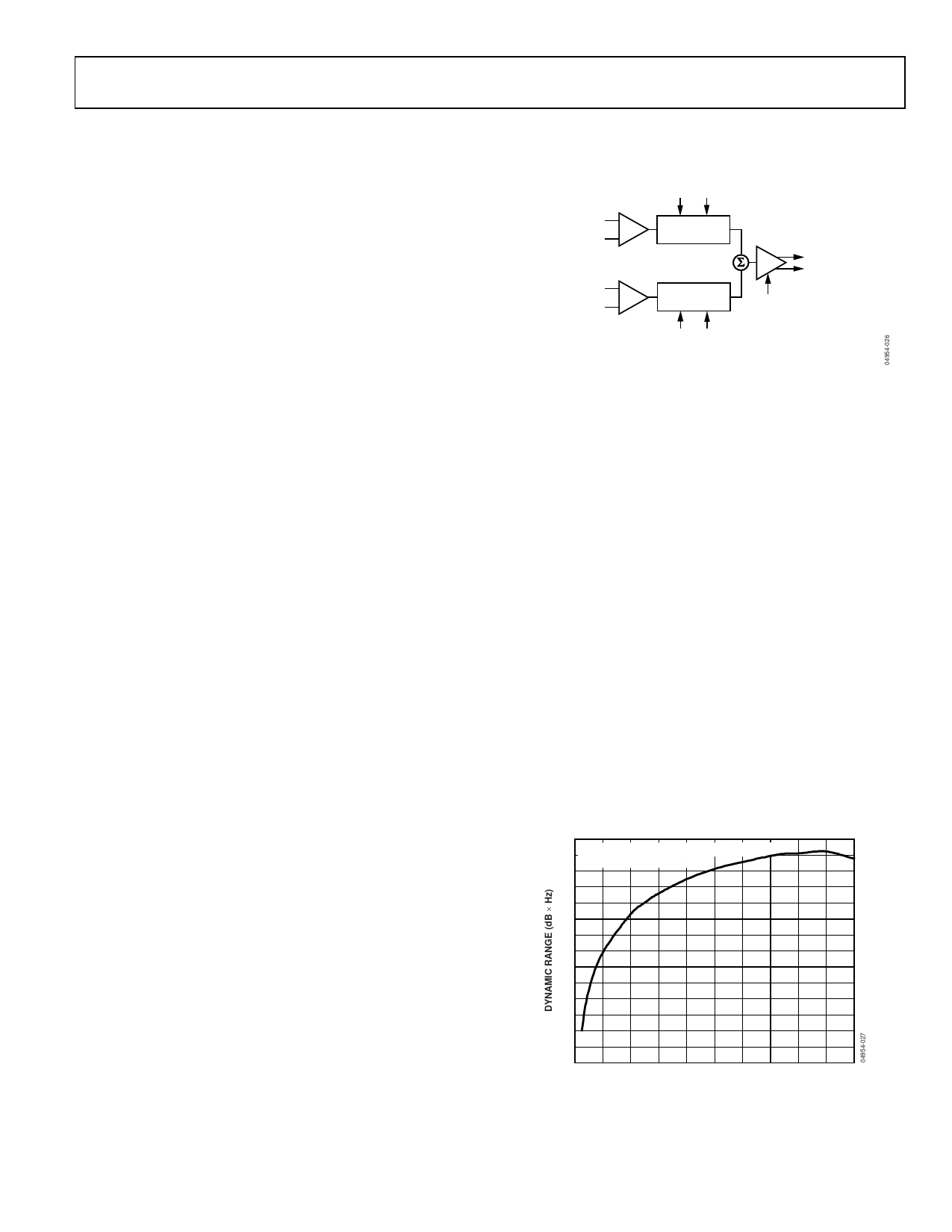
GENERAL STRUCTURE
THEORY OF OPERATION
The simplified block diagram given in Figure 26 shows a
matched pair of variable gain channels whose outputs are
summed and presented to the final output. The RF/IF signals
propagate from the left to the right, while the baseband gain
controls are placed above and below. The proprietary linear-
responding variable attenuators offer excellent linearity, low
noise, and greater immunity from mismatches than other
commonly used methods.
Since the two independent RF/IF inputs can be combined in
arbitrary proportions, the overall function can be termed
“vector multiplication” as expressed by
VOUT = VIRF × (VIBB/VO) + VQRF × (VQBB/VO)
where:
VIRF and VQRF are the RF/IF input vectors.
VIBB and VQBB are the baseband input scalars.
VO is the built-in normalization factor, which is designed to be
0.285 V (1/3.5 V).
The overall voltage gain, in linear terms, of the I and Q channels
is proportional to its control voltage and scaled by the normali-
zation factor, i.e., a full-scale gain of 1.75 (5 dB) for VI (Q)BB of
500 mV. A full-scale voltage gain of 1.75 defines a gain setpoint
of 1.0.
Due to its versatile functional form and wide signal dynamic
range, the ADL5390 can form the core of a variety of useful
functions such as quadrature modulators, gain and phase ad-
justers, and multiplexers. At maximum gain on one channel, the
output 1 dB compression point and noise floor referenced to
50 Ω are 11 dBm and −148 dBm/Hz, respectively. The broad
frequency response of the RF/IF and gain control ports allows
the ADL5390 to be used in a variety of applications at different
frequencies. The bandwidth for the RF/IF signal path extends
from approximately 20 MHz to beyond 2.4 GHz, while the gain
controls signals allow for modulation rates greater than 200 MHz.
Matching between the two gain channels is ensured by careful
layout and design. Since they are monolithic and arranged
symmetrically on the die, thermal and process gradients are
minimized. Typical gain and phase mismatch at maximum gain
are <0.5 dB and <0.5°.
ADL5390
VIRF,
I CHANNEL
SINGLE-ENDED
OR DIFFERENTIAL
VQRF,
Q CHANNEL
SINGLE-ENDED
OR DIFFERENTIAL
I CHANNEL
BASEBAND INPUT
VIBB
V-I
LINEAR
ATTENUATOR
SINGLE-ENDED
I-V
OR DIFFERENTIAL
50Ω OUTPUT
LINEAR
V-I
ATTENUATOR OUTPUT
DISABLE
VQBB
Q CHANNEL
BASEBAND INPUT
Figure 26. Simplified Architecture of the ADL5390
NOISE AND DISTORTION
The signal path for a particular channel of the ADL5390 con-
sists basically of a preamplifier followed by a variable attenuator
and then an output driver. Each subblock contributes some level
of noise and distortion to the desired signal. As the channel gain
is varied, these relative contributions change. The overall effect
is a dependence of output noise floor and output distortion
levels on the gain setpoint.
For the ADL5390, the distortion is always determined by the
preamplifier. At the highest gain setpoint, the signal capacity, as
described by the 1 dB compression point (P1dB) and the third-
order intercept (OIP3), are at the highest levels. As the gain is
reduced, the P1dB and OIP3 are reduced in exact proportion.
At the higher gain setpoints, the output noise is dominated by
the preamplifier as well. At lower gains, the contribution from
the preamplifier is correspondingly reduced and eventually a
noise floor, set by the output driver, is reached. As Figure 27
illustrates, the overall dynamic range defined as a ratio of OIP3
to output noise floor remains constant for the higher gain
setpoints. At some gain level, the noise floor levels off and the
dynamic range degrades commensurate with the gain reduction.
175
DYNAMIC RANGE = OIP3 – (OUTPUT NOISE
FLOOR (NO CARRIER))
170
165
160
155
150
145
140
0
0.1 0.2 0.3 0.4 0.5 0.6 0.7 0.8 0.9 1.0
GAIN SETPOINT
Figure 27. Dynamic Range Variation with Gain Setpoint
Rev. 0 | Page 11 of 24
Share Link: 