CXA1616N Ver la hoja de datos (PDF) - Sony Semiconductor
Número de pieza
componentes Descripción
Lista de partido
CXA1616N Datasheet PDF : 20 Pages
| |||
CXA1616N/S
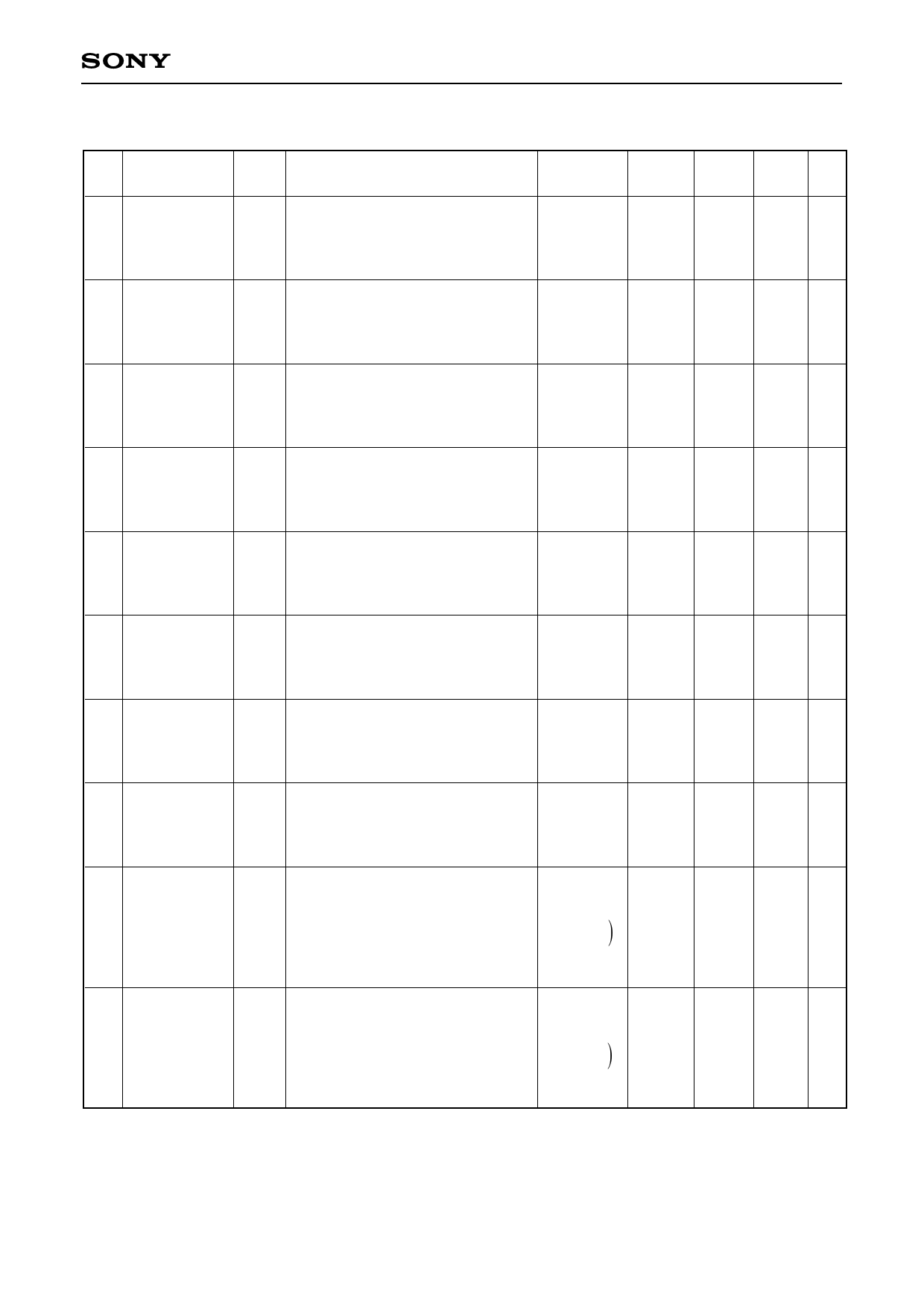
(Ta = 25°C, VCC = 12V, See the Electrical Characteristics Test Circuit)
No.
Item
Symbol
Measurement description
Measure- Min.
ment point
The voltage integral of the vertical
11
PVC voltage 1 VPV1
polarity discrimination circuit for
VS (vertical separate sync) input.
PVC
(Pin 2)
—
Input signal F (negative logic).
The voltage integral of the vertical
12
PVC voltage 2 VPV2
polarity discrimination circuit for
VS (vertical separate sync) input.
PVC
(Pin 2)
—
Input signal G (positive Iogic).
The voltage integral of the vertical
13
PHC voltage 1 VPH1
polarity discrimination circuit for
CS (composite sync) input.
PHC
(Pin 5)
—
Input signal H (negative logic).
The voltage integral of the vertical
14
PHC voltage 2 VPH2
polarity discrimination circuit for
CS (composite sync) input.
PHC
(Pin 5)
—
Input signal I (positive logic).
Measures the voltage of the vertical
15
EVC voltage 1 VEV1
ramp waveform generator for
VS (vertical separate sync) input.
EVC
(Pin 3)
—
Input signal A.
Measures the voltage of the vertical
16
EVC voltage 2 VEV2
ramp waveform generator for
VS (vertical separate sync) input.
EVC
(Pin 3)
—
No input signal.
Measurers the sync existence
17
EHC voltage 1 VEH1
discrimination voltage for
CS (composite sync) input.
Input signal J.
EHC
(Pin 6)
—
Measures the sync existence
18
EHC voltage 2 VEH2
discrimination voltage for
CS (composite sync) input.
No input signal.
EHC
(Pin 6)
—
Measures the delay difference
between CS and HD for
HD
19 HD delay 1
td1
( CS (composite sync) Input. The
time from the CS (negative polarity)
fall time (50%) to the HD output
Pin 18
Pin 20
120
rise time (50%). Input signal B.
Measures the delay difference
20 HD delay 2
td2
between CS and HD for
CS (composite sync) input. The
time from the CS (positive polarity)
rise time (50%) to the HD output
HD
( Pin 18
Pin 20
120
rise time (50%). Input signal D.
Typ. Max. Unit
0.3 — V
3.4 — V
0.4 — V
3.4 — V
7.9 — V
4.3 — V
4.8 — V
3.0 — V
190 250 ns
205 260 ns
–8–
Share Link: 